Alignment Deviation
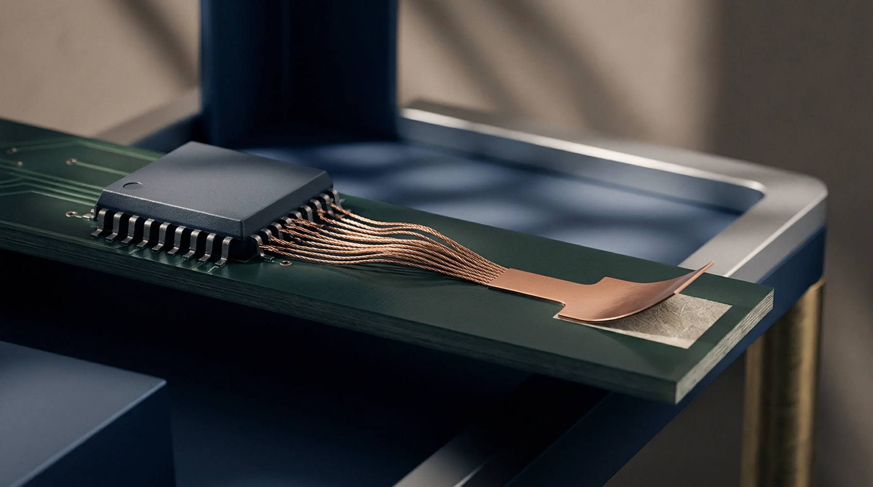
Photolithographic feature positioning occurs through the relative displacement of successive conductive layers during printed circuit board fabrication. Registration shift describes the quantitative offset between the nominal design coordinate and the actual etched position of a copper feature on an inner layer. Manufacturers verify this value by comparing the deviation of fiducial markers against established design tolerances.
Variations exceeding these limits create open circuits or degraded signal integrity through partial connectivity at via pads.
Layer Variance
Production processes introduce mechanical stress that causes substrate expansion or contraction after copper etching. Material instability forces designers to define specific annular ring requirements to accommodate the expected registration shift. Automated optical inspection equipment detects these discrepancies by measuring the distance between drilled holes and circular copper pads.
Small errors remain acceptable provided the resulting solder joint meets defined performance criteria. Precise control of the lamination cycle minimizes the thermal expansion coefficients that drive such positional errors.
Assembly Effect
Secondary misalignment during the solder mask application or component placement phase alters the final contact area on the circuit board. Solder bridges form when registration shift moves a pad too close to an adjacent conductive path or a ground plane. Technicians quantify the impact by performing cross-sectional analysis to verify the remaining copper overlap within the through-hole structure.
Excessive displacement forces the rejection of entire production lots to prevent latent failures in the field. Constant monitoring of tooling holes ensures the consistent location of features across high-density interconnect designs.