Measurement Technology
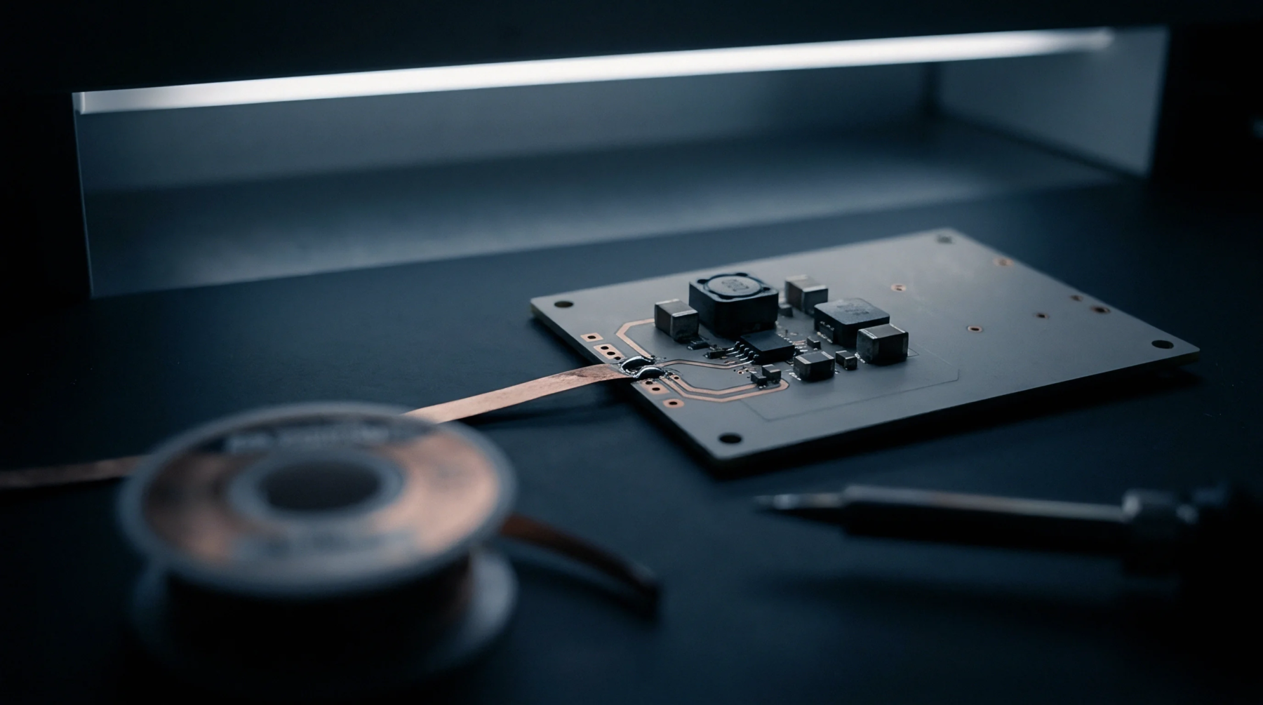
Structured light projection determines the three-dimensional topography of printed solder deposits and mounted components. Automated inspection equipment utilizes phase-shift profilometry to measure the volume, height, and area of deposited solder bricks on the printed circuit board. The instrument projects a series of sinusoidal grating patterns onto the board surface and captures the deformed patterns with a high-resolution camera.
This optical deformation is analyzed to reconstruct a high-precision height map of each pad. By comparing these values to the stencil aperture volumes, the system identifies dry joints or excess solder before component placement.
Optoelectronic Principle
Light patterns are generated by a digital micromirror device and shifted by fractions of the fringe wavelength across the inspection area. When the flat board and the raised solder paste deflect these light fringes, the sensor records the spatial phase difference. Sophisticated algorithms convert these phase differences into absolute height measurements with sub-micron resolution.
Defect Prevention
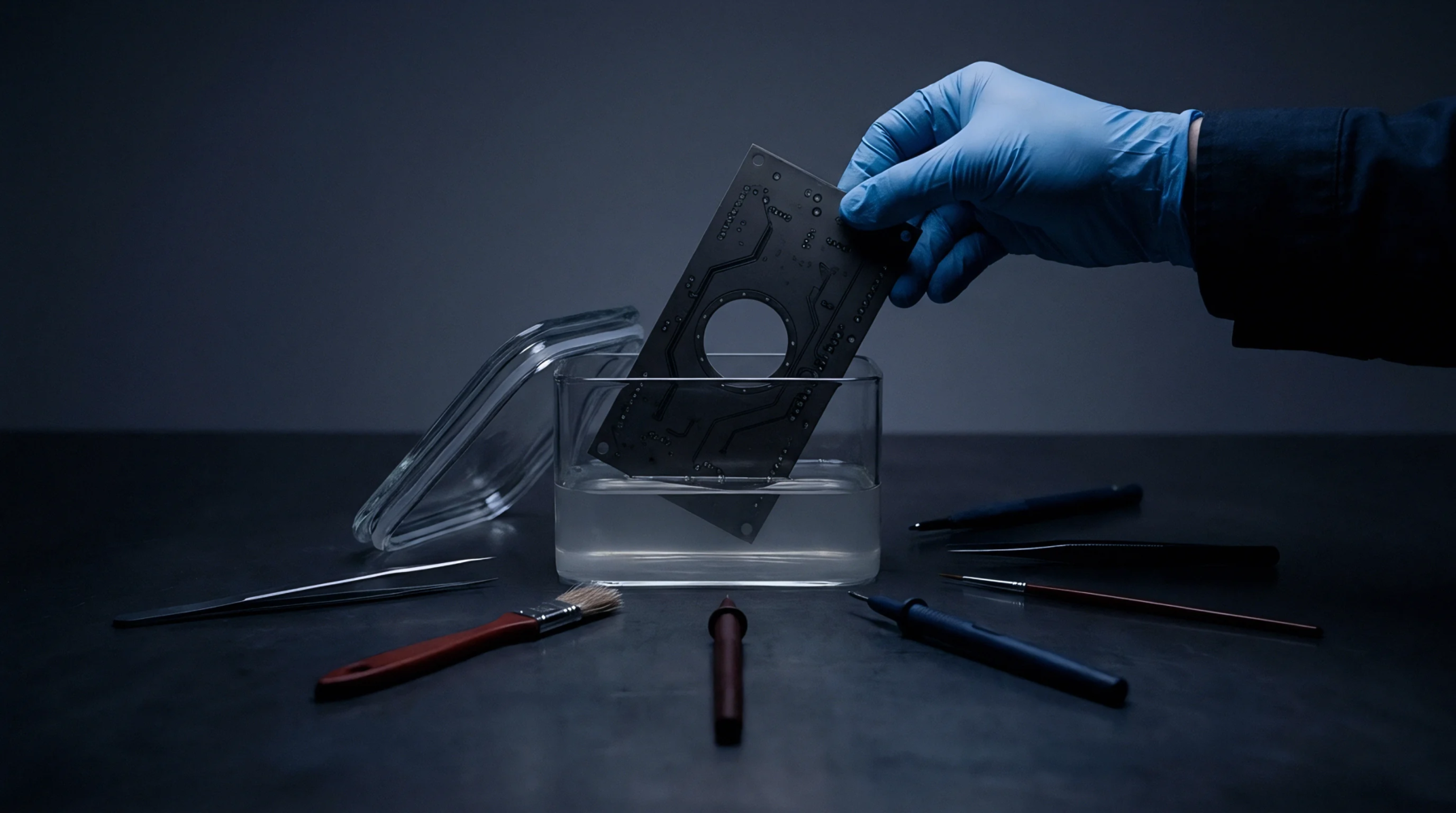
Printed boards that do not meet the volume requirements are routed to a cleaning station for solder reclamation. By identifying low-volume deposits early, the assembly line prevents the formation of open circuits or weak solder joints during the reflow process. This automated inspection step reduces rework costs and improves the overall first-pass yield of the assembly line.