
Ground via Spacing Requirements for Printed Circuit Shielding
Maintain ground via spacing below one-twentieth of dielectric wavelength to prevent slot leakage and pass radiated emissions testing.
Maintain ground via spacing below one-twentieth of dielectric wavelength to prevent slot leakage and pass radiated emissions testing.

Thermally induced crystallization of amorphous nickel phosphide creates non-linear yield drops driven by Ni3P precipitation strain and interfacial cracking.

Sub-tier material drift erodes high-reliability board margins; mathematical risk modeling and rigorous chemical dossier validation eliminate latent field escapes.

Microvia resin filling depends on vacuum timing before viscosity minimum to maximize capillary drive and dissolve trapped bubbles before thermoset gelation.

Multilayer power distribution field escape risk requires bench near-field scanning and transfer impedance limits to prevent far-field compliance chamber failures.
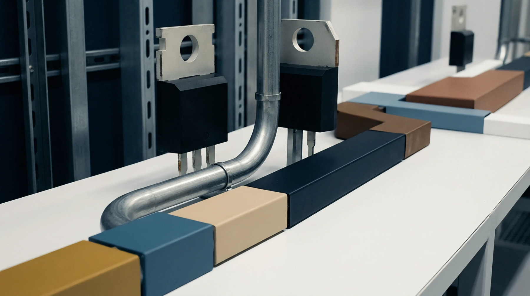
Standard electrical tests verify bare substrate isolation, component pin continuity, thermal stress survival, and electromagnetic conformity before batch signoff.
Expertise is a utility, not a secret. sentiention™ publishes its working knowledge as open reference: intelligence layer covering the materials it sources, the markets it enters, and the reference that serves both.