Ground via Spacing Requirements for Printed Circuit Shielding
Maintain ground via spacing below one-twentieth of dielectric wavelength to prevent slot leakage and pass radiated emissions testing.


Pitch
Radiated field suppression across printed circuit boundaries relies on spacing ground stitching vias at distances significantly smaller than the shortest wavelength of interest. Electromagnetic energy propagates through dielectric substrates at velocities determined by the relative permittivity of the PCB material. When high-speed signal traces or internal radio frequency circuits emit electromagnetic radiation, ground via arrays act as conductive barriers that reflect or absorb incoming fields.
Distance governs attenuation.
The classical electromagnetic guideline specifies placing ground vias at intervals equal to or less than one-tenth of the guided wavelength. High-frequency RF designs and stringent electromagnetic compatibility targets require tighter pitch criteria. Suppressing high-frequency coupling and maintaining isolation above 40 decibels demands via spacing scaled to one-twentieth or one-fiftieth of the guided wavelength.
The guided wavelength calculation incorporates substrate permittivity according to the relation:
lambda_g = c / (f sqrt(epsilon_r))
Where c represents the speed of light in vacuum, f denotes the maximum operational or harmonic frequency, and epsilon_r signifies the relative dielectric constant of the laminate.
| Target Attenuation (dB) | Wavelength Fraction | Spacing at 10 GHz in FR-4 (mm) | Spacing at 24 GHz in FR-4 (mm) |
|---|---|---|---|
| 20 | lambda / 10 | 1.46 | 0.61 |
| 40 | lambda / 20 | 0.73 | 0.30 |
| 60 | lambda / 50 | 0.29 | 0.12 |
| 80 | lambda / 100 | 0.15 | 0.06 |

Empirical Wavelength Scaling for Isolation Fences
Frequency sets wavelength.
Selecting via center-to-center pitch without calculating effective dielectric loading leads to electromagnetic boundary failure. Standard FR-4 epoxy laminate exhibits a relative permittivity near 4.2 at gigahertz frequencies. Hydrocarbon ceramic laminates present lower permittivity values near 3.5, altering the internal spatial wavelength.
Ground via stitching designed for lower frequencies allows higher-order harmonics to slip through unhindered when inter-via distances exceed half the wave interval.
Ground via arrays spacing tighter than one twentieth of the dielectric wavelength convert discrete copper barrels into an effective continuous conductive boundary.
Designers configuring printed circuit board shielding fences balance high-frequency isolation goals against mechanical drilling limitations. Placing ground barrels too close together structural weakens board laminate and risks drill breakthrough during multi-layer fabrication. Ground barrels placed closer than the substrate cut-off dimension turn segmented copper walls into continuous electromagnetic shields.

Leakage
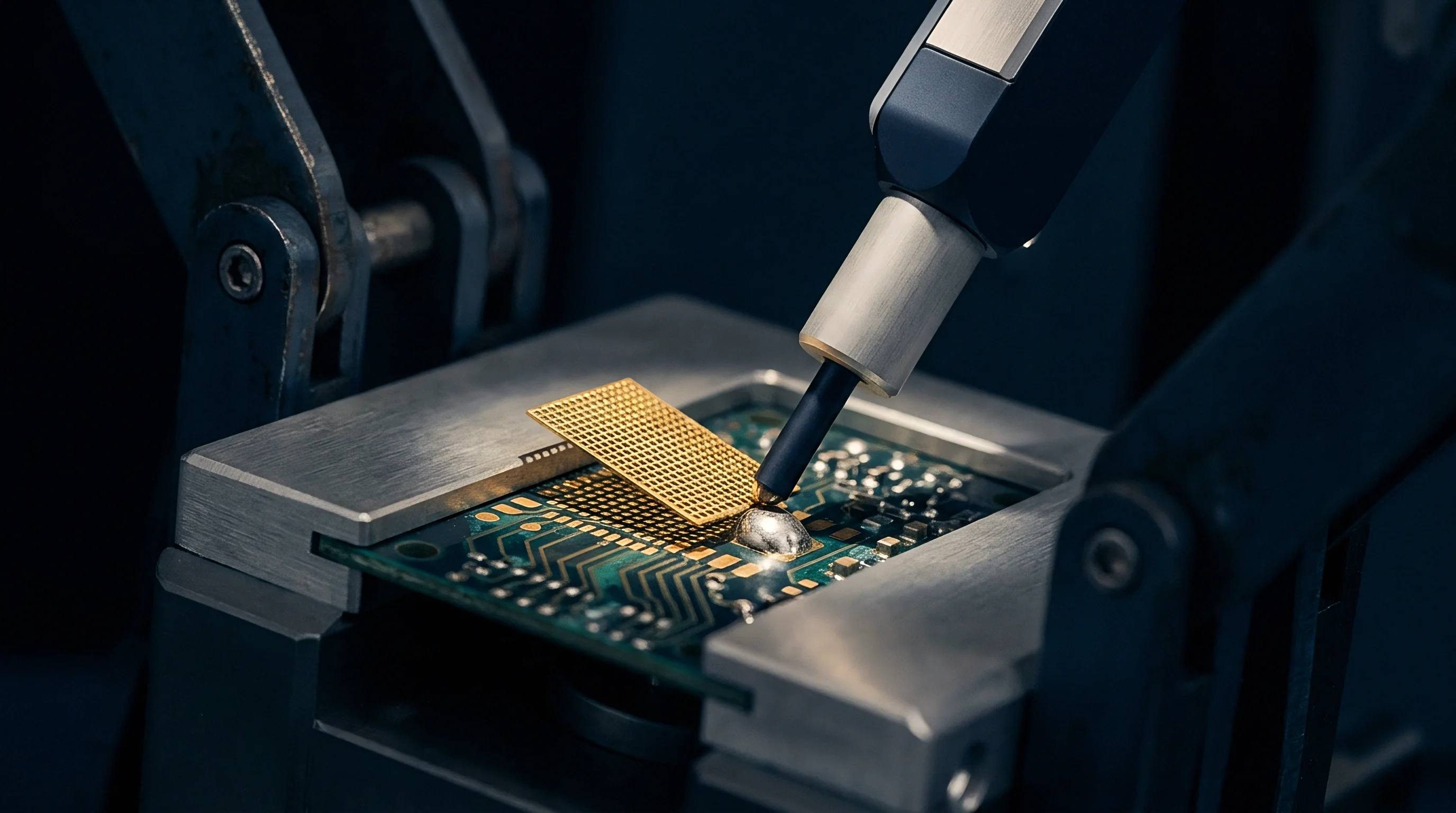
Apertures formed between adjacent via barrels act as slot antennas whenever signal frequencies approach the cut-off frequency of the inter-via gap. Spacing ground vias creates an array of vertical copper cylinders separated by unplated dielectric material. Unshielded dielectric gaps act as waveguides that permit energy transfer across board perimeters.
Slot width dictates leakage.
The cut-off frequency of an aperture formed by two ground vias depends directly on the center-to-center separation distance minus the finished drill diameter. When the physical length of the inter-via slot equals half a wavelength, energy transfers through the barrier with minimal attenuation. The fundamental cut-off frequency for an inter-via aperture is defined by:
f_cutoff = c / (2 g sqrt(epsilon_r))
Where g represents the net edge-to-edge gap between adjacent plated via barrels.

Slot Antenna Formation and Inter via Cut-off
Radiation through guard ring gaps increases rapidly above one-half of the aperture cut-off frequency. Signal harmonics generated by digital switching circuits or power converter drivers leak through board perimeters when via density drops along copper plane edges. Maintaining isolation performance requires keeping inter-via edge distances far below half-wavelength resonance points.
An inter-via spacing of two millimeters in glass-epoxy dielectric creates a slot resonance near thirty-six gigahertz that reduces isolation by twenty decibels.
Edge radiation from multi-layer board stacks creates severe electric field spikes during formal compliance testing. Ground planes terminated without surrounding stitching via rows allow substrate-guided waves to radiate from open PCB board edges into ambient space. Failing to control aperture dimensions turns ground stitching rows into radiating slots during emissions qualification, forcing costly board respins and halting shipment schedules.

Inductance
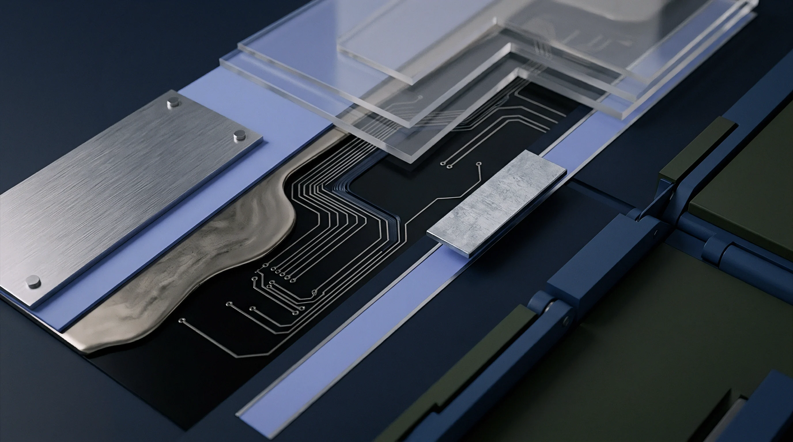
Ground return currents traversing layer transitions encounter localized magnetic field energy storage within the vertical barrel structure. Short signal paths across board layers demand low-impedance ground return paths immediately adjacent to signal vias. High via loop inductance causes ground bounce, localized voltage fluctuations, and signal degradation across high-speed interconnects.
Return currents seek low impedance.
The total parasitic inductance of a vertical ground via barrel relates directly to its physical height and drill diameter. Thicker boards and smaller drill diameters increase total vertical barrel inductance according to standard physical approximations:
L_via = (mu_0 h / (2 pi)) (ln(4 h / d) + 1)
Where h represents board layer transition height, d denotes finished drill diameter, and mu_0 signifies magnetic permeability of free space.
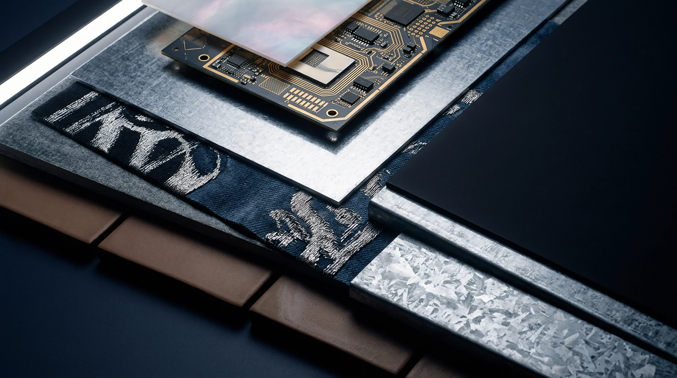
Barrel Parasitics and Return Path Discontinuities
Barrel inductance creates voltage drop.
Placing ground stitching vias close to signal layer transitions minimizes loop area and limits magnetic field expansion. High-frequency return currents follow paths of minimum inductance rather than minimum resistance. When a ground via sits too far from a high-speed signal transition, return currents travel wide loops across ground planes, radiating RF energy into neighboring traces.

Why Do High Frequency Shielding Boundaries Require Double Row via Arrays?
Single stitching lines leave inductive loops between individual barrels that allow high-frequency magnetic fields to breach boundary planes. Staggering two parallel rows of ground vias reduces total path inductance through parallel path sharing and creates an overlapping physical barrier against radiated waves.
- Single row aperture radiation creates periodic electric field leakage points across high-speed plane boundaries when operating near gigahertz frequencies.
- Staggered array cancellation reduces inter-barrel slot coupling by blocking direct line-of-sight energy transmission pathways through substrate gaps.
- Ground bounce buildup drops significantly when multiple parallel vertical copper paths lower local power ground distribution impedance.
- Anti-pad overlap slotting destabilizes continuous ground reference planes, requiring immediate surrounding via clusters to maintain loop control.
High-frequency modeling continues to debate whether staggered dual-row via arrays provide measurable shield enhancement over single-row arrays when trace anti-pads disrupt ground plane continuity.


Plating
High via density along shielding perimeters places severe physical demands on PCB fabrication processes during mechanical drilling and wet-process copper deposition. Placing ground holes too close together causes laminate cracking, resin recession, and plating voids between adjacent barrel walls. Fabricators enforce minimum spacing rules to prevent manufacturing defects and ensure long-term interconnect reliability.
Drill wander reduces annular margins.
Drill bit deflection occurs when mechanical drill bits traverse multi-layer stacks at high feed rates. Close via pitch layout heightens the risk of drill bits wandering into adjacent copper barrels, causing inner-layer short circuits or barrel wall breakouts. Maintaining sufficient copper web thickness between drilled holes prevents mechanical fractures during laminate thermal expansion.
| Fabrication Parameter | IPC-6012 Class 2 Standard | IPC-6012 Class 3 High Reliability | Impact on Shield Pitch Layout |
|---|---|---|---|
| Minimum Plating Thickness | 20 micrometers | 25 micrometers | Determines high-frequency current carrying capacity |
| Minimum Web Distance | 0.20 millimeters | 0.25 millimeters | Sets physical lower limit for inter-via drill spacing |
| Annular Ring Breakout | 90 degree max breakout | Zero breakout allowed | Requires larger via capture pad diameters |
| Target Drill Clearance | 0.25 millimeters | 0.30 millimeters | Dictates maximum achievable shielding via density |

Mechanical Stress and Barrel Integrity
Thermal fatigue breaks thin copper.
Repeated thermal cycling causes z-axis expansion inside glass-epoxy board substrates. Dense rows of ground vias experience cumulative shear stress along copper barrel walls during thermal shock testing. Inadequate copper plating thickness combined with tight via spacing leads to circumferential barrel cracking and intermittent ground connection loss under field operation.
Compliance with IPC-6012 Class 3 annular ring rules prevents circumferential barrel cracking during repeated thermal cycling across automotive temperature ranges.
To ensure robust mechanical manufacturing while maintaining high electromagnetic shielding efficacy, assembly engineers rely on rigid design verification steps:
- Minimum drill pitch limit enforces safe spatial clearance between adjacent hole edges to prevent laminate micro-fracturing during high-speed mechanical drilling operations.
- Annular ring retention allowance provides sufficient outer-layer copper coverage around drilled holes to guarantee full circumferential pad connectivity after registration variations.
- Capture pad expansion factor scales inner-layer ground plane connection areas to withstand thermal expansion forces without tearing away from plated barrel walls.
- Thermal stress screening window Subjects finished test coupons to thermal solder float testing to reveal latent barrel plating separation before batch assembly release.
Fabricators frequently claim that high via density along edge plating paths causes localized resin recession and micro-voiding beyond their standard process control limits.

Proof
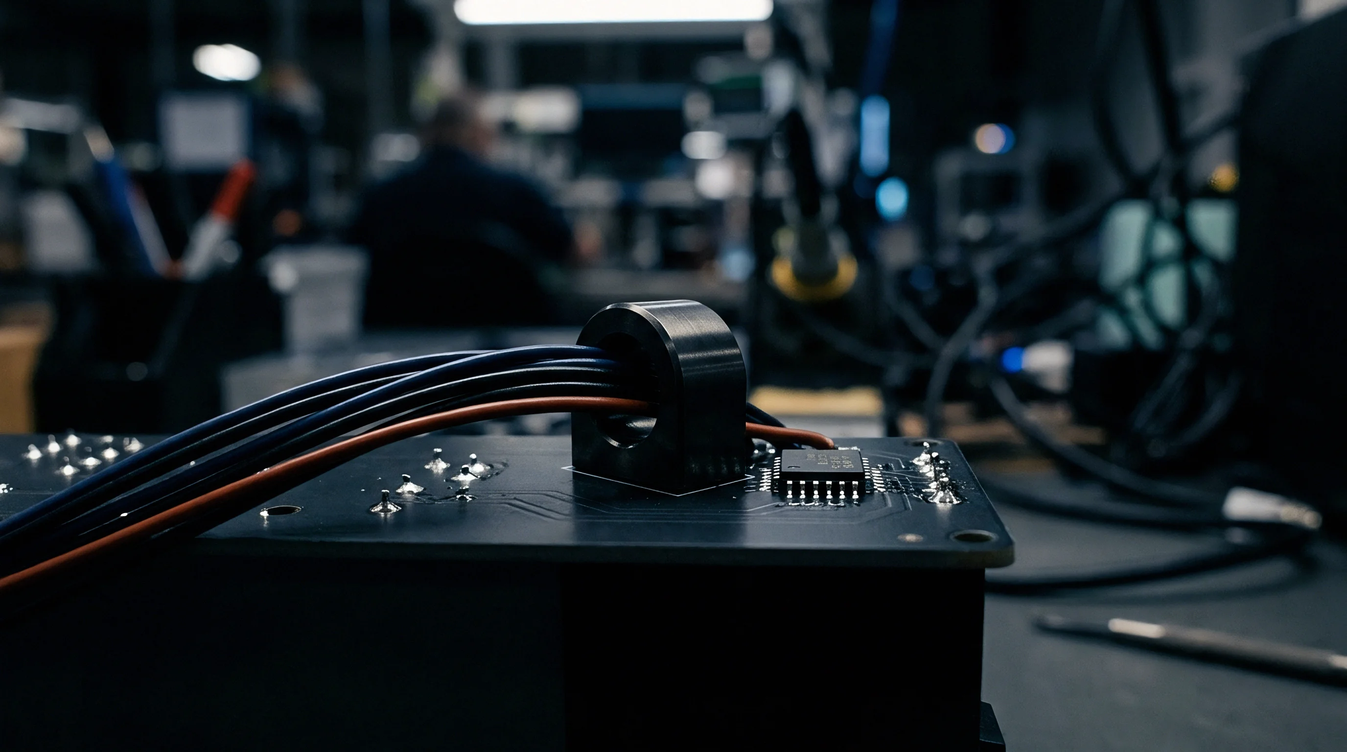
Demonstrating shielding effectiveness requires direct physical measurement across near-field and far-field electromagnetic test environments. Automated near-field magnetic probe scanners evaluate electric and magnetic leakage across ground via fences before final enclosure design commitment. Transmission loss measurements verify isolation performance across targeted spectrum bands.
Near-field probe mapping pinpoints inter-via slot radiation long before far-field chamber testing detects an emissions breach.
Testing verifies isolation limits.
Near-field probes reveal slot radiation.
Standardized measurement protocols on dedicated test coupons isolate via array effectiveness from external cable or connector coupling effects. Vector network analyzers measure insertion loss parameters across microstrip structures bounded by ground via arrays. Quantitative attenuation maps confirm whether a given ground via spacing meets specified isolation targets under real-world operating conditions.

Verification Procedures for via Shield Performance
Chamber time increases project cost.
Quantifying ground via array attenuation on physical test coupons follows a strict laboratory execution sequence:
- Calibrate vector network analyzer port cables across the designated frequency sweep range.
- Connect microstrip launch probes to adjacent shielded RF channels on the unpopulated coupon.
- Record baseline transmission loss across open reference board structures without ground via fences.
- Measure transmission loss across boards featuring specified via fence pitch layouts.
- Calculate net shielding effectiveness by subtracting reference loss values from via fence loss values across the target spectrum.
Shielding failures halt market release.
Field returns ruin batch margin.
Compliance holds clear customs borders. Documenting compliance with international electromagnetic compatibility directives relies on verified laboratory test reports. Citing EN 55032 Class B limits in purchase orders obligates suppliers to verify ground via stitching effectiveness before final product declaration.

Warranty
Unresolved electromagnetic interference escaping poorly stitched board perimeters converts directly into post-delivery financial liabilities during commercial market surveillance. Regulatory authorities regularly perform random market sampling, testing electronic hardware for compliance with radiated emissions limits. Non-compliant hardware faces immediate sales bans, customs holds, and mandatory field recalls.
Poor layout causes signal crosstalk.
The financial cost of improper ground via layout far exceeds the board fabrication expenditure. Re-engineering an unshielded printed circuit layout due to regulatory failure triggers expensive re-qualification cycles, chamber re-testing fees, and missed production launch windows. Sourcing practices protect commercial margins by demanding full electromagnetic compatibility verification reports prior to high-volume manufacturing sign-off.
Suppliers delivering assemblies that fail radiated emissions benchmarks bear full financial responsibility for board scrap, re-spinning costs, and expedited freight charges. Incorporating proven ground via spacing rules during initial layout verification eliminates regulatory rejection risks and guarantees commercial compliance across global markets.