Finite Element Shear Failure Modeling for Latent Interface Cracking in High Temp Thermal Aging
Finite element shear modeling predicts latent interface cracking in high-temperature electronics by applying age-degraded cohesive zone parameters.
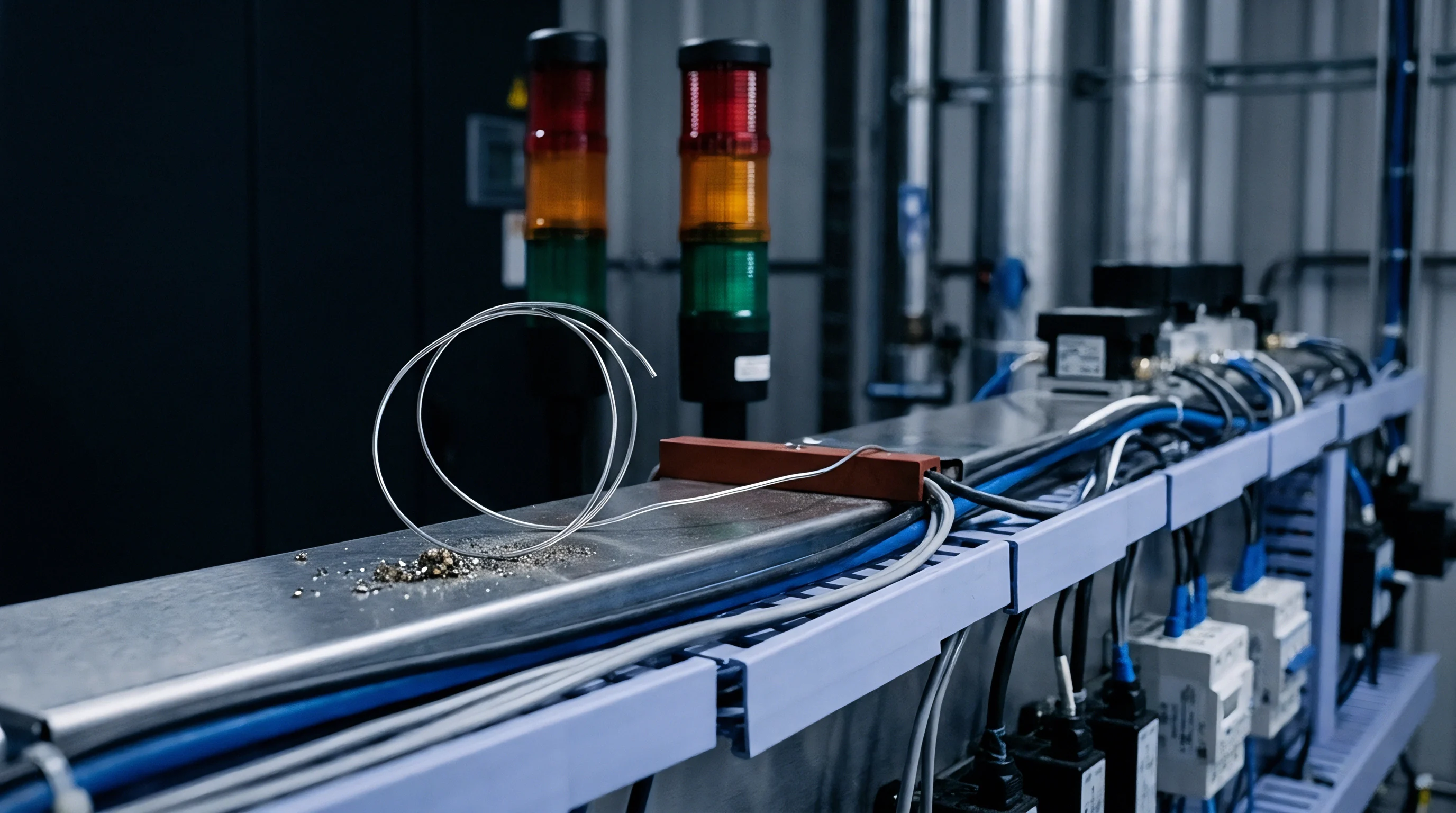
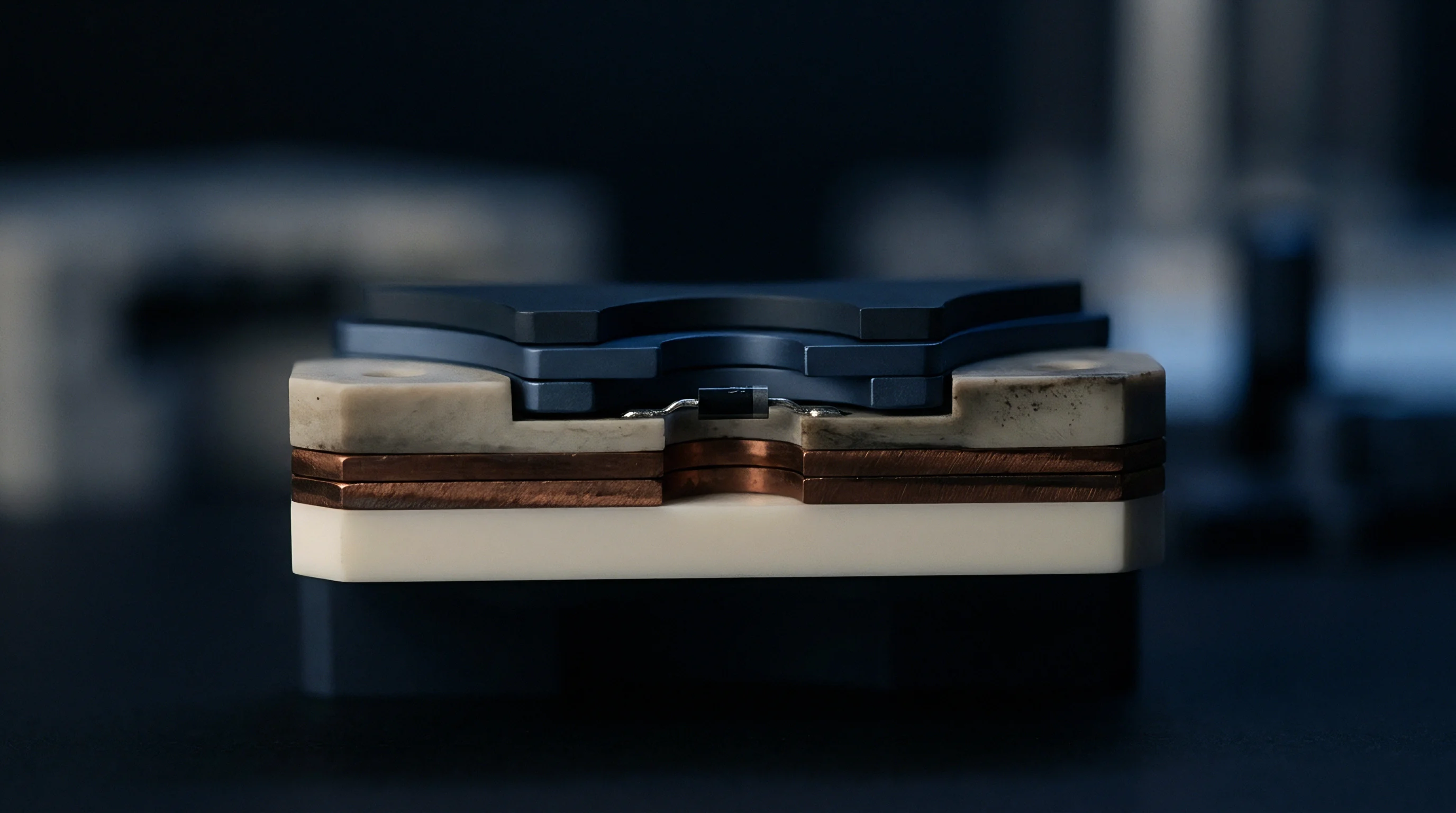
Seam
Integrated circuit packages subjected to prolonged isothermal storage experience internal stress shifts along the boundary separating metallic pads from polymer encapsulation or solder alloys. Silicon dies, substrate laminates, and molding compounds expand at different rates during continuous operation above 125 degrees Celsius. The mismatch in thermal expansion coefficients drives concentrated forces across flat bonding surfaces.
Microscopic separations develop invisibly during initial thermal cycles, remaining completely undetectable under standard optical or low-frequency functional tests. When operational loads generate transient mechanical shock or localized expansion, these pre-existing internal microcracks propagate rapidly, severing electrical connections.
Interface stresses accumulate quietly. Finite element modeling isolates these planar boundaries to predict structural breakdown before field deployment. The primary difficulty stems from the changing material states within the metallic joints during continuous heating.
Copper atoms diffuse into tin-based solders, forming brittle intermetallic compound layers such as copper-three-tin and copper-six-tin-five. As these compound zones grow, their fracture energy drops, transforming a ductile stress absorber into a brittle cleavage plane. Finite element simulations that assume static material properties underpredict shear failure probability by several orders of magnitude.

Subsurface Microstructural Degradation at BGA Interfaces
Intermetallic growth consumes pure copper from board traces and component leads, creating microscopic voids through Kirkendall Kirkendall-type vacancy coalescence. High temperature bake profiles maintained at 150 degrees Celsius for 1000 hours induce structural changes that weaken the bond line. The elastic modulus of the intermetallic zone rises to roughly 110 gigapascals, while the surrounding solder matrix softens under thermal stress relaxation.
This mechanical contrast forces applied shear displacement directly into the thin intermetallic seam. Microcracks initiate at sharp pad corners where stress concentration factors reach maximum values.
- Intermetallic Growth Phase High temperature exposure converts soft solder alloys into rigid intermetallic compounds, concentrating shear strains along a planar zone less than five micrometers thick.
- Kirkendall Void Aggregation Vacancy movement toward the copper surface generates sub-micrometer cavities that coalesce into structural continuous failure lines under cyclic shear loading.
- Matrix Creep Softening Solder material surrounding the bond area loses yield strength, eliminating plastic energy dissipation and transferring shear displacement to brittle interface layers.
- Encapsulant Moisture Release Outgassing of trapped resin volatiles creates localized vapor pressure pockets that push die attachment boundaries apart during thermal excursions.

Thermal Activation of Intermetallic Shear Weakening
Diffusion rates follow exponential temperature dependence, accelerating interfacial alteration at high operating temperatures. Mathematical representations of this behavior combine Fickian diffusion equations with continuum damage mechanics. When numerical models neglect the progressive growth of brittle intermetallic layers, predicted failure modes stay artificially ductile.
Silicon contracts faster than substrate resin. Physical cross-sections cut through aged ball grid arrays reveal clean planar separations along the copper-intermetallic boundary rather than plastic deformation through the bulk solder ball.
Contract manufacturing facilities often explain field returns after high-temperature bake testing by claiming that incoming component batches contained improper metallization plating thickness. This explanation routinely ignores the localized shear stress state caused by thermomechanical strain mismatch across large silicon die footprints during thermal qualification screens.

Formulation
Numerical simulation of latent interface failure relies on cohesive zone elements placed directly along potential fracture paths. Standard continuum elements fail to capture the sharp displacement jump that occurs when two bonded materials uncouple under tangential displacement. Placing zero-thickness cohesive elements between substrate copper pads and solder ball interfaces allows finite element solvers to calculate localized damage accumulation.
The constitutive framework couples normal stress and shear stress through a bi-linear or exponential traction-separation formulation.
Damage evolution rules monitor energy dissipation during mechanical loading. Pure mode-two shear displacement drives pure sliding, while mixed-mode conditions combine tensile lifting with lateral sliding. High temperature exposure alters critical fracture energy values, shifting the failure threshold downward as bake time increases.
Incorporating degradation parameters into finite element modeling software guarantees accurate prediction of crack initiation locations under board-level bending or temperature cycling.

Cohesive Zone Modeling for Bilayer Separation
Simulating structural degradation requires explicit definition of normal and shear stiffness parameters prior to crack initiation. Elastic moduli for cohesive elements are set sufficiently high to prevent artificial flexibility in the assembly before damage begins. Damage starts when interfacial shear stress reaches the ultimate interfacial shear strength.
Once stress crosses this limit, element stiffness degrades linearly or exponentially toward zero, simulating progressive bond failure.
Cohesive element stiffness must be set two orders of magnitude higher than surrounding continuum elements to prevent numerical compliance artifacts prior to damage initiation.
Executing accurate interface shear failure simulations requires a precise sequence of preprocessing and parameter mapping steps within the finite element solver setup environment.
- Construct geometry with coincident node pairs along the target metallization bond boundary.
- Insert zero-thickness cohesive elements between adjacent continuum solid elements across the interface plane.
- Define directional penalty stiffness values matching physical substrate rigidity.
- Input temperature-dependent interfacial shear strength and normal yield stress derived from experimental shear testing.
- Assign mixed-mode power-law fracture criteria linking mode-one opening and mode-two sliding energy rates.
- Apply nodal thermal expansion field gradients reflecting actual chamber ramp conditions.
- Solve thermal-stress equilibrium equations using non-linear Newton-Raphson iteration.
- Export scalar damage variables to verify crack front progression across the component footprint.

Mixed Mode Traction Separation Law Execution
Mode-two shear fracture energy dominates interface failure when board warping induces lateral displacement across ball grid array joints. Under pure mode-two shear, cohesive elements accumulate damage based on critical tangential displacement. Combining shear deformation with mode-one tensile peeling accelerates material breakdown according to a Benzeggagh-Kenane power-law relationship.
As temperature increases, critical fracture toughness drops nonlinearly.
| Bake Time at 150°C (Hours) | Interfacial Shear Strength (MPa) | Mode II Fracture Toughness J/m² | Initial Shear Stiffness (MPa/mm) | Damage Initiation Strain Factor |
|---|---|---|---|---|
| 0 (Unaged) | 52.4 | 142.0 | 1.2 x 10^6 | 0.0042 |
| 250 | 41.1 | 98.5 | 1.1 x 10^6 | 0.0035 |
| 500 | 33.8 | 65.2 | 9.4 x 10^5 | 0.0028 |
| 1000 | 22.5 | 31.0 | 7.8 x 10^5 | 0.0019 |
Fracture toughness drops under heat. The degradation rates captured in material property tables allow finite element software to predict exact failure initiation zones across high-density interconnect designs. Transient stress spikes that cause zero damage on unaged boards will trigger complete interface separation after five hundred hours of thermal conditioning.
How does the non-linear interaction between copper-tin intermetallic growth and dynamic stress relaxation affect numerical convergence in implicit finite element solvers?

Aging
High temperature conditioning destabilizes metallic microstructures, lowering the mechanical work necessary to separate material interfaces. Elevated temperatures accelerate atom diffusion across the joint line, forming intermetallic compounds that possess higher hardness but significantly lower impact resistance. Thermal stress relaxation simultaneously reduces peak shear stresses in bulk solder, transferred load concentrates along the rigid intermetallic boundary.
This mechanism hides structural degradation, as macro-level stress relaxation masks microscopic embrittlement.
Diffusion kinetics follow standard Arrhenius relations, doubling intermetallic reaction rates for specific temperature steps. At ambient operating temperatures, interfacial changes progress slowly over years. In contrast, burn-in operations and high-temperature storage tests conducted between 125 and 150 degrees Celsius drive interface evolution within weeks.
Finite element simulations incorporating age-dependent constitutive damage laws accurately predict the resulting drop in shear capacity.

Arrhenius Constitutive Softening in Solder Joint Matrix
Constitutive model formulation requires updating matrix yield parameters based on accumulated thermal exposure hours. Anand creep model constants, widely used for lead-free solder alloys, change continuously as grain coarsening occurs during isothermal conditioning. Activation energy values dictate how fast the material loses resistance to plastic deformation under sustained mechanical shear strain.
Testing under JESD22-A103 condition B at 150 degrees Celsius for 1000 hours reduces shear strength at copper-solder interfaces by more than fifty percent due to intermetallic phase conversion.
Modulus reduction in the bulk solder shifts structural compliance during thermal cycling. While a softer solder matrix reduces peak normal stress caused by global thermal expansion mismatch, it allows larger lateral shear displacement. This increased shear displacement concentrates mechanical strain inside the rigid intermetallic seam, accelerating localized microcrack formation.
Intermetallic Layer Thickness and Critical Fracture Toughness
Intermetallic growth rates govern interface brittle behavior. Unaged solder joints maintain thin intermetallic layers under one micrometer, exhibiting high resistance to shear failure. After prolonged high-temperature storage, intermetallic layer thickness routinely exceeds four micrometers.
Critical mode-two fracture energy decreases monotonically as this intermetallic thickness increases, lowering the threshold for rapid crack propagation.
Copper drives intermetallic growth. Structural durability specifications like IPC-9701 require component qualification through controlled thermal cycling following elevated temperature storage. When supply contracts exclude explicit intermetallic thickness caps after post-bake qualification, assembly buyers assume full commercial responsibility for latent field delamination.

Shear
Physical measurement of interfacial structural capacity validates finite element cohesive models. High-speed ball shear tests and cold bump pull methods quantify force required to fracture individual solder interconnects. Performing shear tests on components subjected to varying bake durations yields empirical traction-separation curves.
Test fixtures must hold substrate boards rigid to eliminate parasitic bending moments that artificially lower measured shear forces.
High temperature ball push mechanics reveal brittle failure modes undetectable at room temperature. Testing joints at operating temperatures of 105 degrees Celsius ensures that matrix softening effects do not mask interfacial embrittlement. Comparing finite element failure predictions against physical load-displacement curves confirms model accuracy across different thermal aging intervals.
Has Acoustic Microscopy Resolved Subsurface Delamination Prior to Destructive Shear Testing?
Scanning acoustic microscopy detects density changes at material boundaries, revealing subsurface delamination before mechanical shear testing occurs. High-frequency ultrasonic transducers operating between 100 MHz and 230 MHz identify internal voiding, interface separation, and molding compound delamination. Acoustic reflection signatures map delamination areas across large die boundaries, providing exact crack size validation data for finite element cohesive zone geometries.
| Test Method | Applicable Standard | Defect Resolution | Sample Type | Destructive State |
|---|---|---|---|---|
| High-Speed Ball Shear | JESD22-B117 | 1.0 µm Displacement Jump | Individual Joint | Destructive |
| C-Mode Acoustic Microscopy | IPC/JEDEC J-STD-035 | 5.0 µm Planar Delamination | Full Board / Package | Non-Destructive |
| Micro-Section Sectioning | IPC-TM-650 2.1.1 | 0.1 µm Intermetallic Thickness | Coupled Joint Section | Destructive |
| 4-Point Bend Shear Load | IPC-9702 | 10.0 µm Crack Extension | Board Level Assembly | Destructive |
Fixture alignment dictates test accuracy. Precision alignment prevents angular misorientation during shear tool contact, eliminating parasitic vertical forces that alter shear stress calculations. Microcracks initiate at sharp corners when tool height offsets exceed ten percent of total solder bump height.
Contractual acceptance under IPC-A-610 Class 3 mandates zero internal delamination exceeding fifteen percent of total pad contact area following environmental stress screening.
Cold Lap and High Temperature Ball Push Mechanics
Testing shear performance across elevated temperatures isolates the specific contribution of intermetallic layers from that of the bulk solder matrix. Room temperature shear testing often forces fracture through the soft solder bulk, obscuring underlying interface weaknesses. High temperature shear testing reduces bulk solder strength, allowing the tool to measure true interfacial adhesion under thermal load.
- High-Speed Tool Shear Pushing solder bumps at velocities above 100 millimeters per second forces brittle failure along the intermetallic layer, exposing latent bond flaws.
- Temperature-Controlled Fixture Clamp Securing test vehicles inside a thermal chamber during shear force measurement ensures data matches actual operational board temperatures.
- Ductile-to-Brittle Transition Mapping Recording fracture mode transitions across aging intervals provides empirical damage evolution metrics for numerical solver calibration.
- Post-Shear Fracture Scanning Electron microscopy analysis of exposed pad surfaces quantifies percentage of intermetallic cleavage relative to ductile solder tear zones.
Latent flaws bypass visual checks. Relying solely on room-temperature mechanical testing leads directly to field escapes, where assemblies experience catastrophic interface separation under modest thermomechanical vibration.
Exposure
Unmitigated latent interface cracking presents substantial financial risk for high-reliability electronics deployments. Component lots passing initial production screening can fail prematurely in service as operating heat accelerates intermetallic growth. Warranties covering automotive, aerospace, or industrial computing equipment carry heavy financial penalties when root causes trace back to preventable interface delamination.
Finite element shear modeling establishes predictable life limits, enabling accurate warranty reserve calculations.
Yield losses spike without warning. Integrating validated cohesive zone simulations into preliminary design routines identifies high-risk component layouts prior to tooling release. Adjusting copper pad geometries, trace fanouts, and underfill materials mitigates localized shear concentrations, lowering long-term field return rates.
Quantifying Field Warranty Reserves for Latent Delamination
Calculating financial reserve requirements relies on cumulative damage distribution curves generated from cohesive finite element models. Weibull analysis converts simulated failure time distributions into expected field failure rates over multi-year service horizons. When models show crack initiation occurring within standard product warranty windows, engineering teams modify thermal management designs or mandate upgraded interconnect metallization.
Margin calculations absorb structural risk. Setting financial reserves based on unaged solder strength parameters leaves organizations exposed to massive recall expenditures when high-temperature operational environments degrade bond strength.
Batch Release Criteria under Thermomechanical Degradation
Quality assurance protocols require integrating finite element failure limits into lot release criteria. Production samples subjected to accelerated thermal aging bakes undergo high-speed shear verification before batch sign-off. When measured shear forces drop below model-derived thresholds, entire component lots face quarantine to prevent field escapes.
Validating interface integrity before product release protects operational capital and satisfies strict regulatory audit mandates. Combining predictive finite element shear modeling with rigorous physical verification creates a complete technical dossier capable of withstanding market authority audits.
Components specified for extended high temperature service require qualification against aged cohesive zone fracture limits rather than baseline unaged mechanical shear values.