Printed Circuit Board Differential Trace Impedance Test Methods
Differential trace impedance testing verifies high-speed PCB signal integrity using time-domain reflectometry on panel test coupons.
Differential trace impedance testing verifies high-speed PCB signal integrity using time-domain reflectometry on panel test coupons.
Subtractive etch factor variations along trace runs create localized impedance drift and coherent reflection peaks that severely degrade high frequency return loss.
Trapezoidal trace tapering reduces effective line width, raising microstrip impedance above rectangular model predictions and demanding field solver validation.
Quantify anisotropic permittivity drift by extracting tensor components across environmental chambers to preserve differential impedance and phase margins.
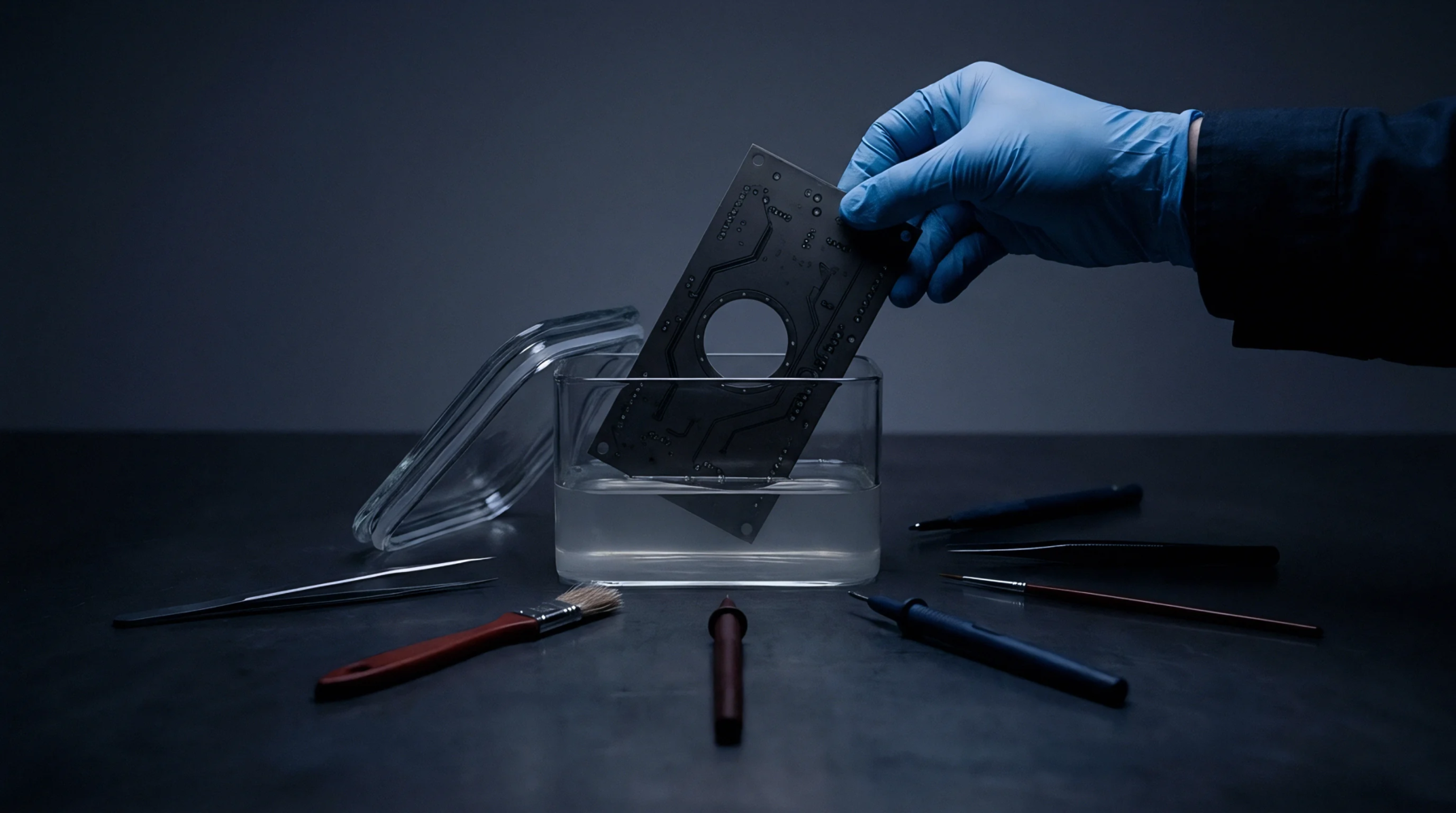
Sub-stack thickness drift stems from secondary resin compression during sequential lamination, requiring flow-controlled prepregs and thieving arrays to hold Z-axis impedance.

Correlating microsection geometry with TDR readings requires adjusting static field solver inputs for trapezoidal trace slope, copper roughness, and frequency-dependent permittivity.
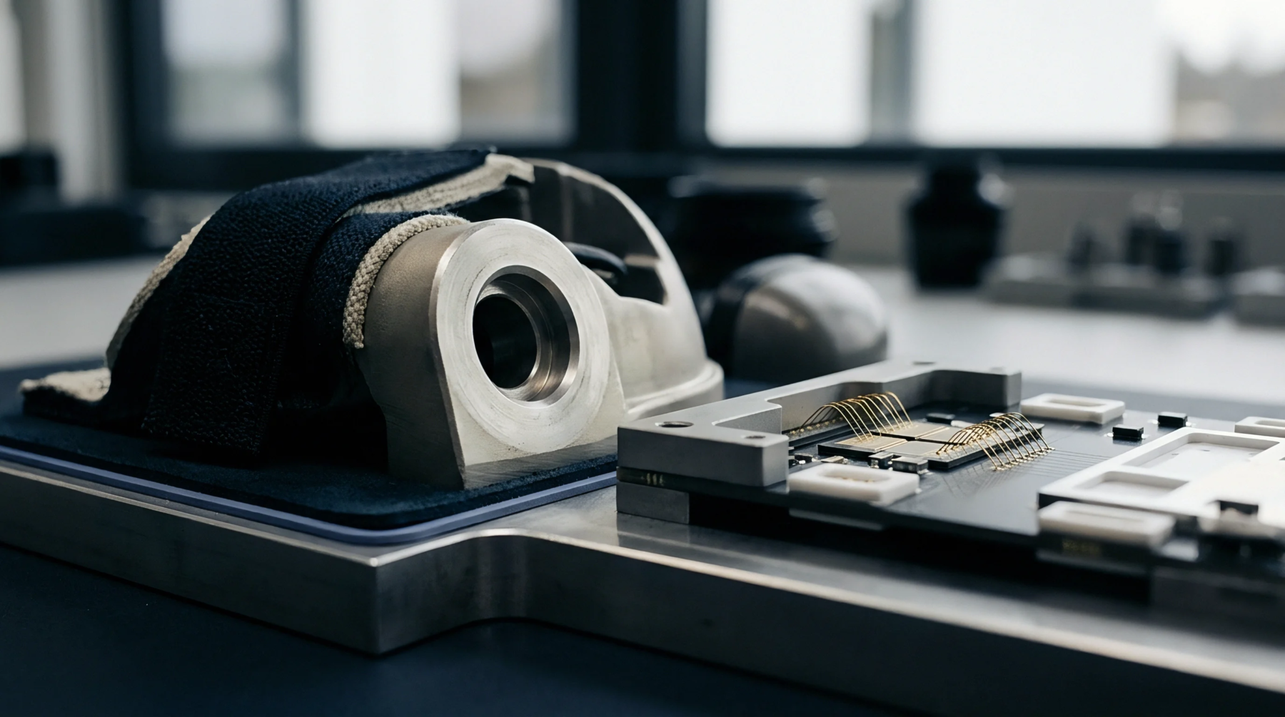
Selecting spread glass fabrics and controlling resin distribution tightens microstrip relative permittivity tolerances, eliminating differential phase skew.

Extracting out-of-plane permittivity requires guarded parallel-plate or re-entrant cavity tests to isolate vertical flux fields from in-plane glass weave effects.
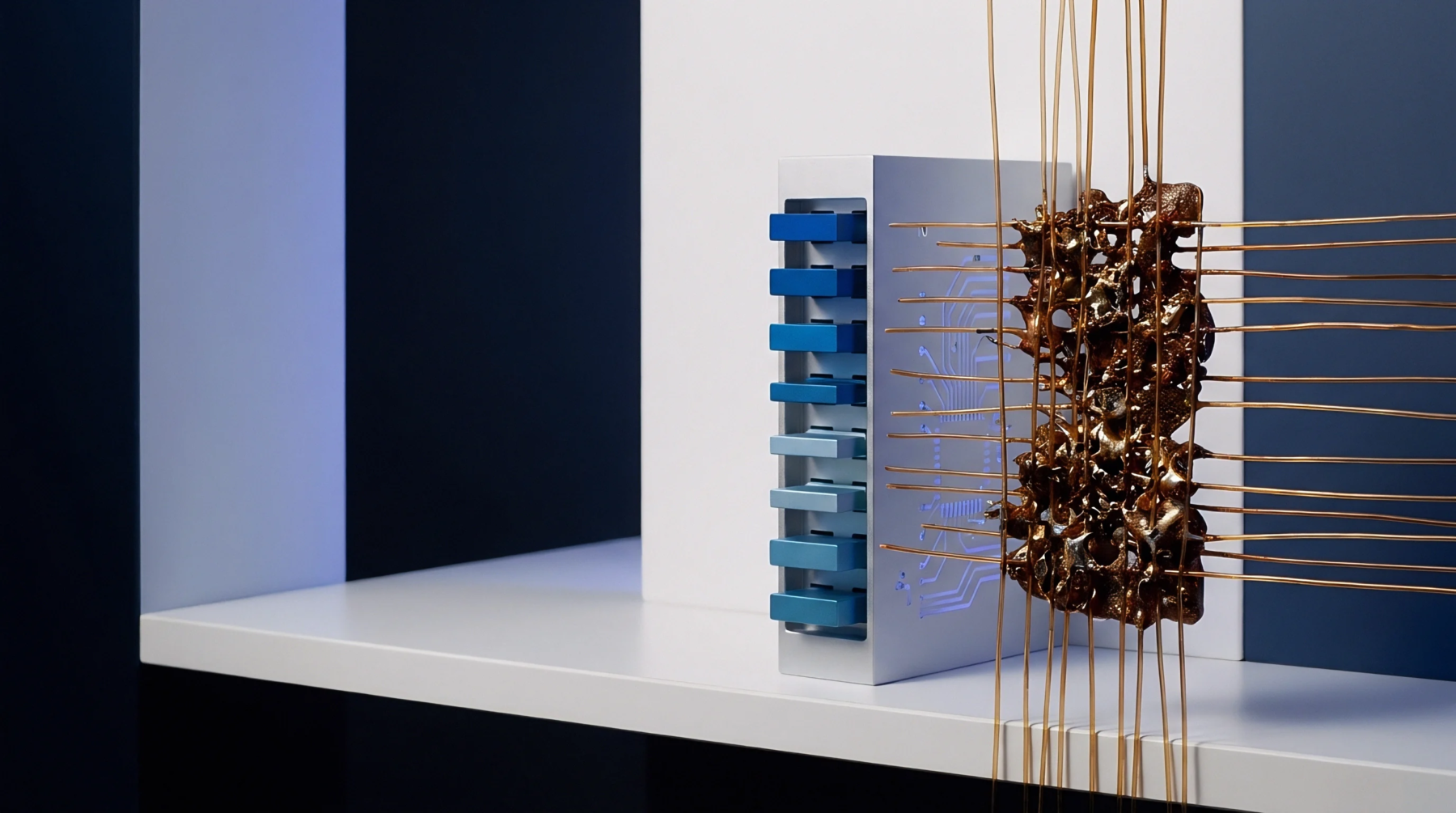
Spatial dielectric variation in glass laminates stems from weave periodicity and drives phase skew, requiring spread glass or angled routing to pass tight jitter budgets.
Expertise is a utility, not a secret. sentiention™ publishes its working knowledge as open reference: intelligence layer covering the materials it sources, the markets it enters, and the reference that serves both.