Printed Circuit Board Differential Trace Impedance Test Methods
Differential trace impedance testing verifies high-speed PCB signal integrity using time-domain reflectometry on panel test coupons.
Differential trace impedance testing verifies high-speed PCB signal integrity using time-domain reflectometry on panel test coupons.
Subtractive etch factor variations along trace runs create localized impedance drift and coherent reflection peaks that severely degrade high frequency return loss.
TDR discontinuity spikes from undercut are quantified by mapping trapezoidal trace profile ratios to TDR reflection peaks filtered at matched rise times.
Ultra-smooth copper reduces boundary wall friction, accelerating resin squeeze-out and requiring tailored lamination press cycles to hold dielectric thickness.
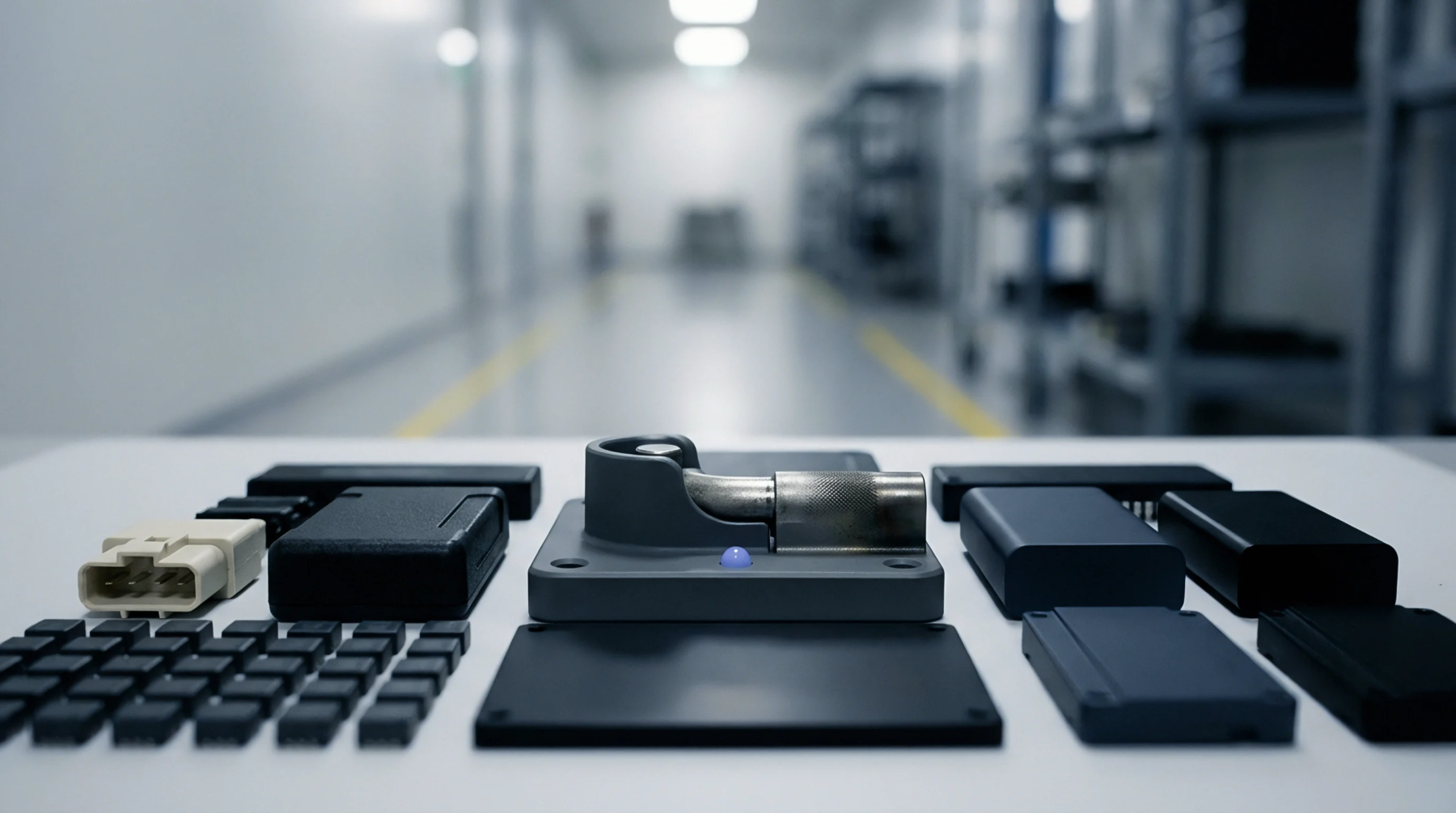
Trapezoidal trace tapering reduces effective line width, raising microstrip impedance above rectangular model predictions and demanding field solver validation.

GHz acoustic attenuation in sub-ten micron dielectric layers limits echo signal-to-noise ratio, requiring picosecond laser acoustics for reliable characterization.
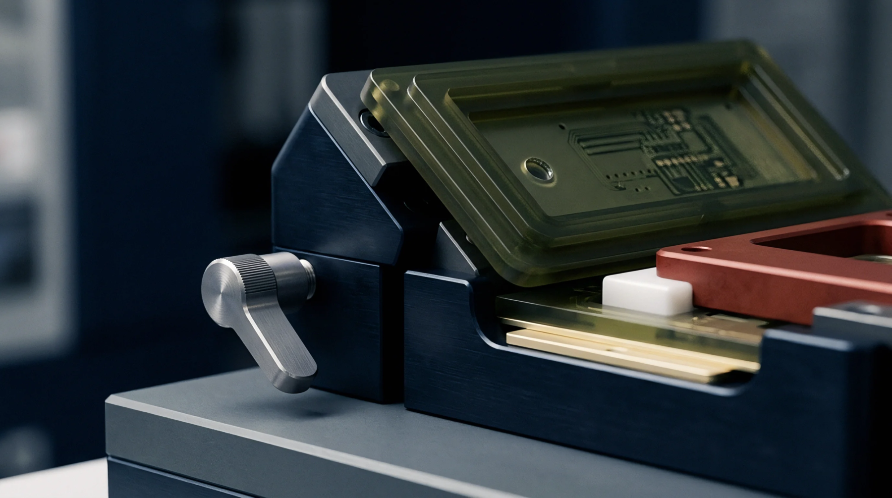
Micro-fractures in high-speed coupling capacitors elevate insertion loss and phase jitter; wideband S-parameter screening catches latent dielectric failures.
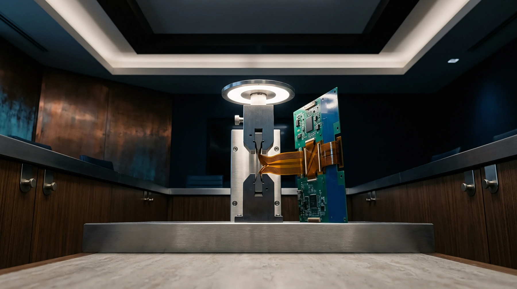
Extracting return path discontinuity metrics requires multi-port VNA s-parameters, IEEE 370 de-embedding, and IFFT conversion to quantify impedance spikes.
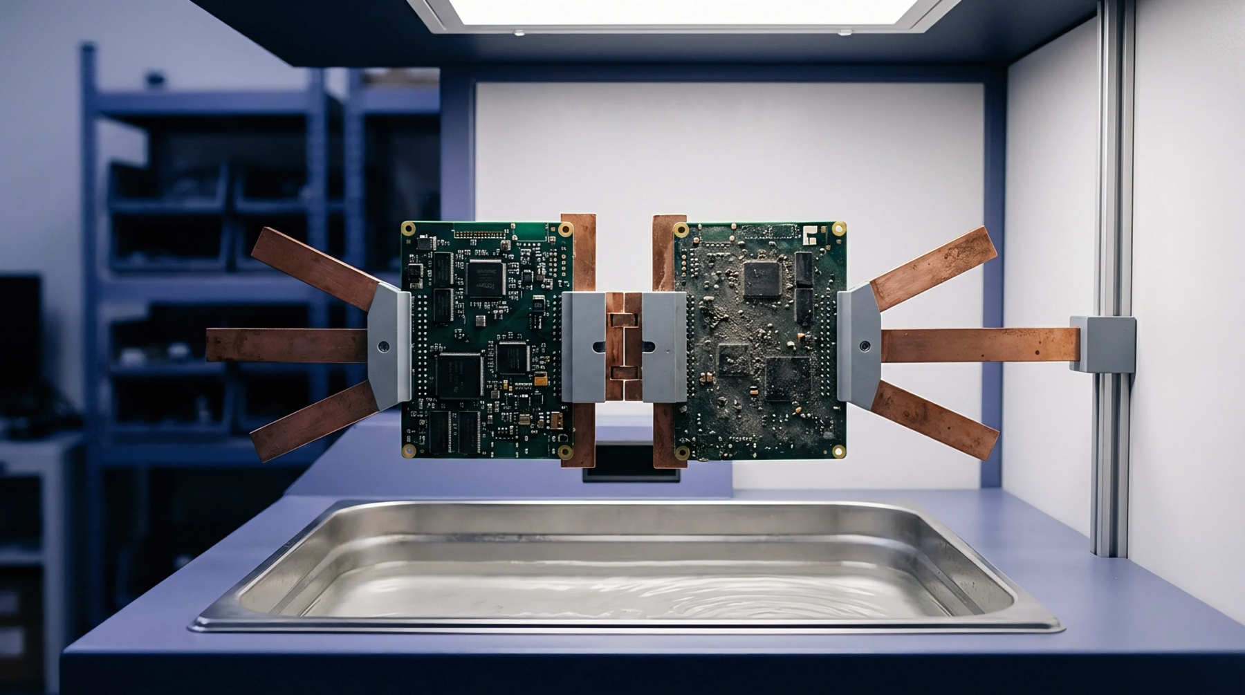
Spread glass styles eliminate dielectric spatial variation, stabilizing differential impedance and phase skew across high-frequency printed circuit routing.
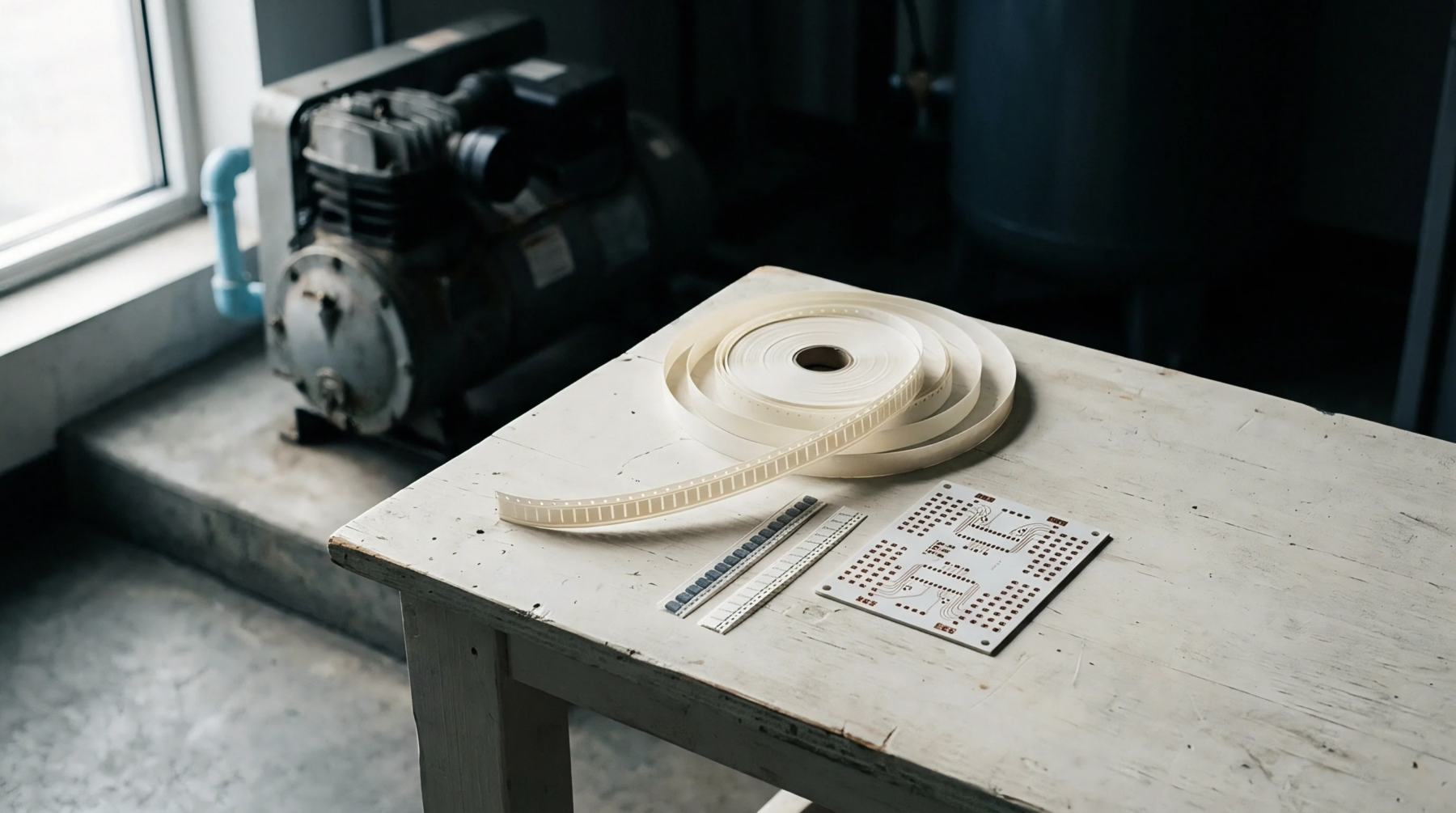
Calculate stripline impedance by applying the geometric mean of in-plane and z-axis permittivity to sidewall fringing fields to eliminate 2-ohm routing offsets.
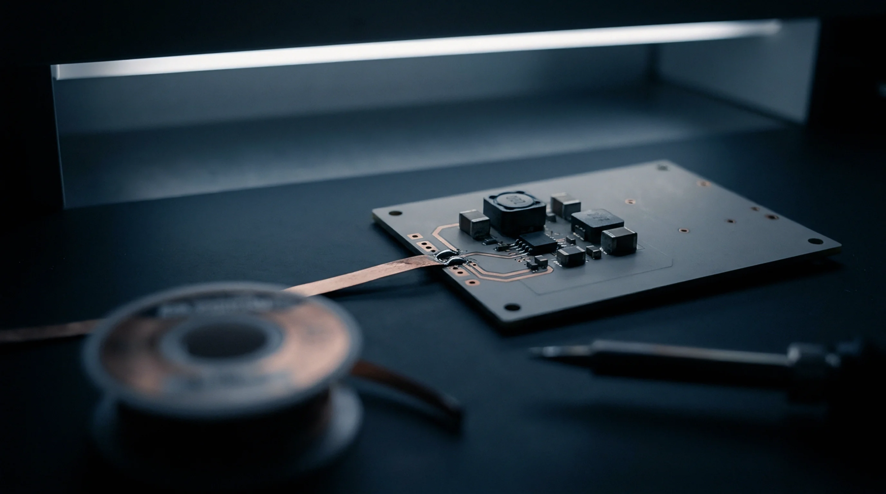
Dynamic thermal gradients alter substrate permittivity, causing severe phase delay skew and PAM4 eye closure unless mitigated by ultra-flat glass and low-drift resins.
Mid-loss laminates balance dissipation factors between 0.005 and 0.010 with moderate panel costs, matching PCIe Gen 4 and 10GbE signal integrity demands.
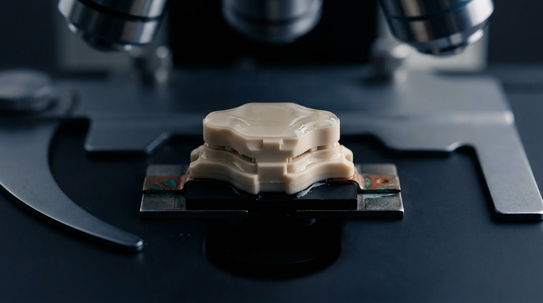
Spatial dielectric variation across organic package cores causes differential phase skew and impedance ripple, requiring spread glass and strict panel-level metrology.
Reconciling static field solvers with TDR curves requires transforming 2D RLGC parameters into causal, broadband S-parameters with instrument rise-time filtering.

Low-frequency DC probing misses high-speed differential symmetry defects, requiring combined TDR, AC scan, and S-parameter metrics to bound structural escapes.
Standardizing microstrip impedance on anisotropic substrates demands tensor permittivity inputs or Schneider equivalence transformations in field solvers.
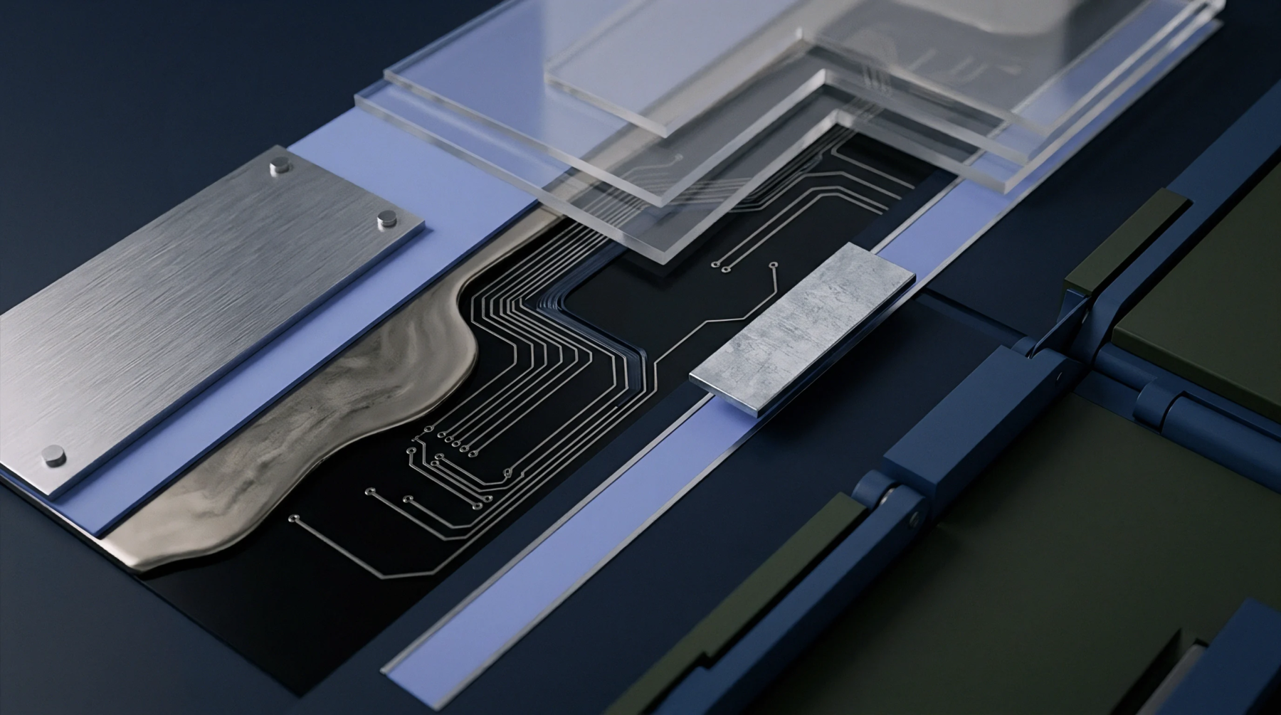
Sequential lamination elevates core dielectric constant through resin cure advancement, requiring pass-specific permittivity modeling to protect target impedance.
Sub-micron interfacial crack growth under high-frequency electromagnetic and thermomechanical stress is driven by local skin-depth current crowding and Maxwell stress tensor concentration.
Expertise is a utility, not a secret. sentiention™ publishes its working knowledge as open reference: intelligence layer covering the materials it sources, the markets it enters, and the reference that serves both.