
Printed Circuit Board Differential Trace Impedance Test Methods
Differential trace impedance testing verifies high-speed PCB signal integrity using time-domain reflectometry on panel test coupons.
Differential trace impedance testing verifies high-speed PCB signal integrity using time-domain reflectometry on panel test coupons.
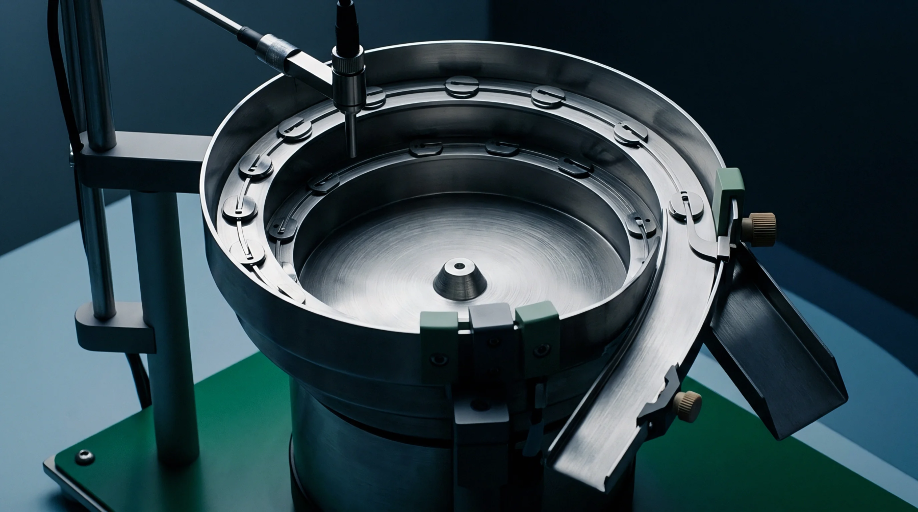
Subtractive etch factor variations along trace runs create localized impedance drift and coherent reflection peaks that severely degrade high frequency return loss.

GHz acoustic attenuation in sub-ten micron dielectric layers limits echo signal-to-noise ratio, requiring picosecond laser acoustics for reliable characterization.

Eliminating high speed ICT escape vectors demands AC boundary scan integration, controlled overdrive pulse timing, and board strain limits during fixture probing.

Finite element analysis verification against physical strain gauge telemetry requires localized mesh refinement and empirical contact friction coefficients.

Thermally induced crystallization of amorphous nickel phosphide creates non-linear yield drops driven by Ni3P precipitation strain and interfacial cracking.
Cyclic thermal loading degrades epoxy shear modulus, causing strain transfer loss that demands strict bondline guard-banding in technical files.

Quantifying aging micro-fractures in high-Q cavities links mechanical strain to Q-drop and out-of-band field escape spectra breaching EMC limits.

Resolving intermittent high speed signal integrity escapes requires pairing static boundary scan with embedded IJTAG at speed stress testing to catch dynamic physical layer failures.

Market surveillance sampling targets high-risk import batches; importers defend compliance through accredited test dossiers and formal uncertainty guard bands.

First pass yield gaps in high-density assemblies stem from optical test blind spots, microvia structural fatigue, and restricted physical probe access.

Integrating hybrid boundary scan and flying probe regimes eliminates unreached structural defects by establishing 99 percent nodal fault coverage.
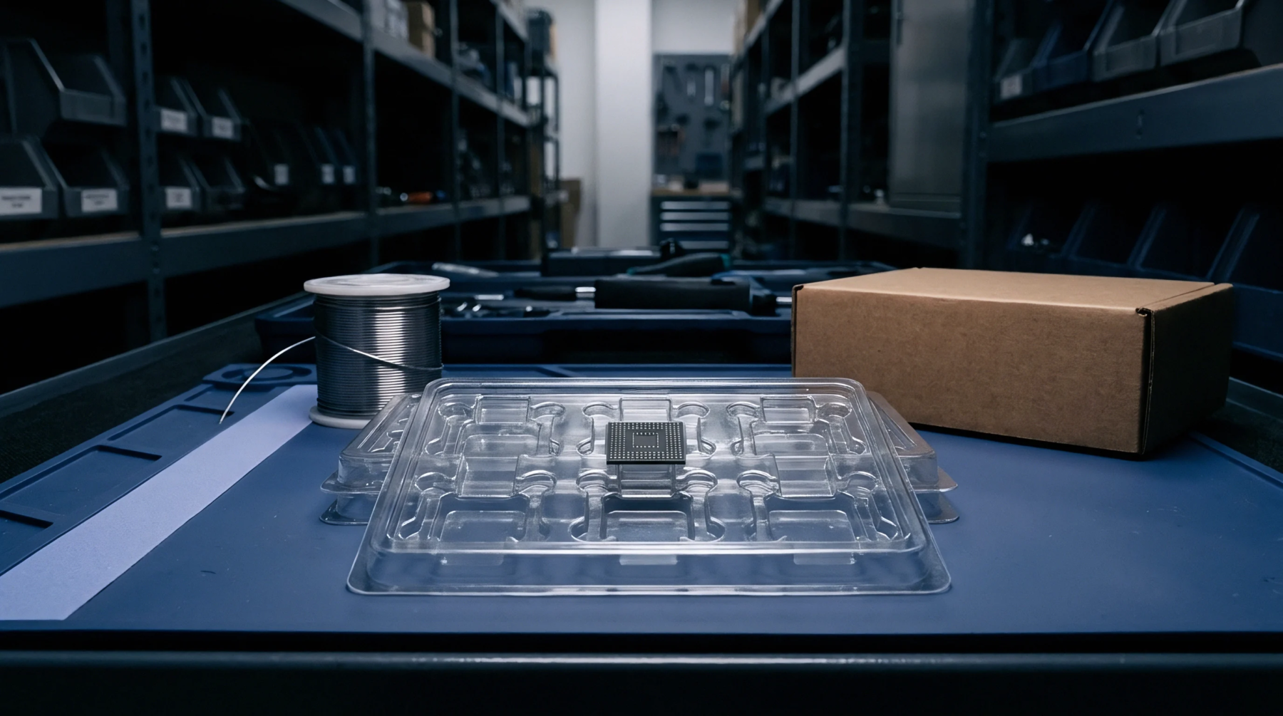
Quantitative depth profiling via AES or XPS accurately measures sub-nanometer interfacial oxidation and phosphorus enrichment to prevent joint failures.

Multilayer power distribution field escape risk requires bench near-field scanning and transfer impedance limits to prevent far-field compliance chamber failures.
Expertise is a utility, not a secret. sentiention™ publishes its working knowledge as open reference: intelligence layer covering the materials it sources, the markets it enters, and the reference that serves both.