Conductive Surface
Electrolytic copper foil with a very smooth treatment on the bonding side minimizes resistive losses at high frequencies. Applying hvlp copper foil to a laminate reduces the skin effect by providing a flatter path for current flow. The acronym stands for hyper very low profile, indicating a surface roughness typically below 1.5 microns.
This material is essential for signal integrity in applications operating above 10 GHz.
Adhesion Mechanism
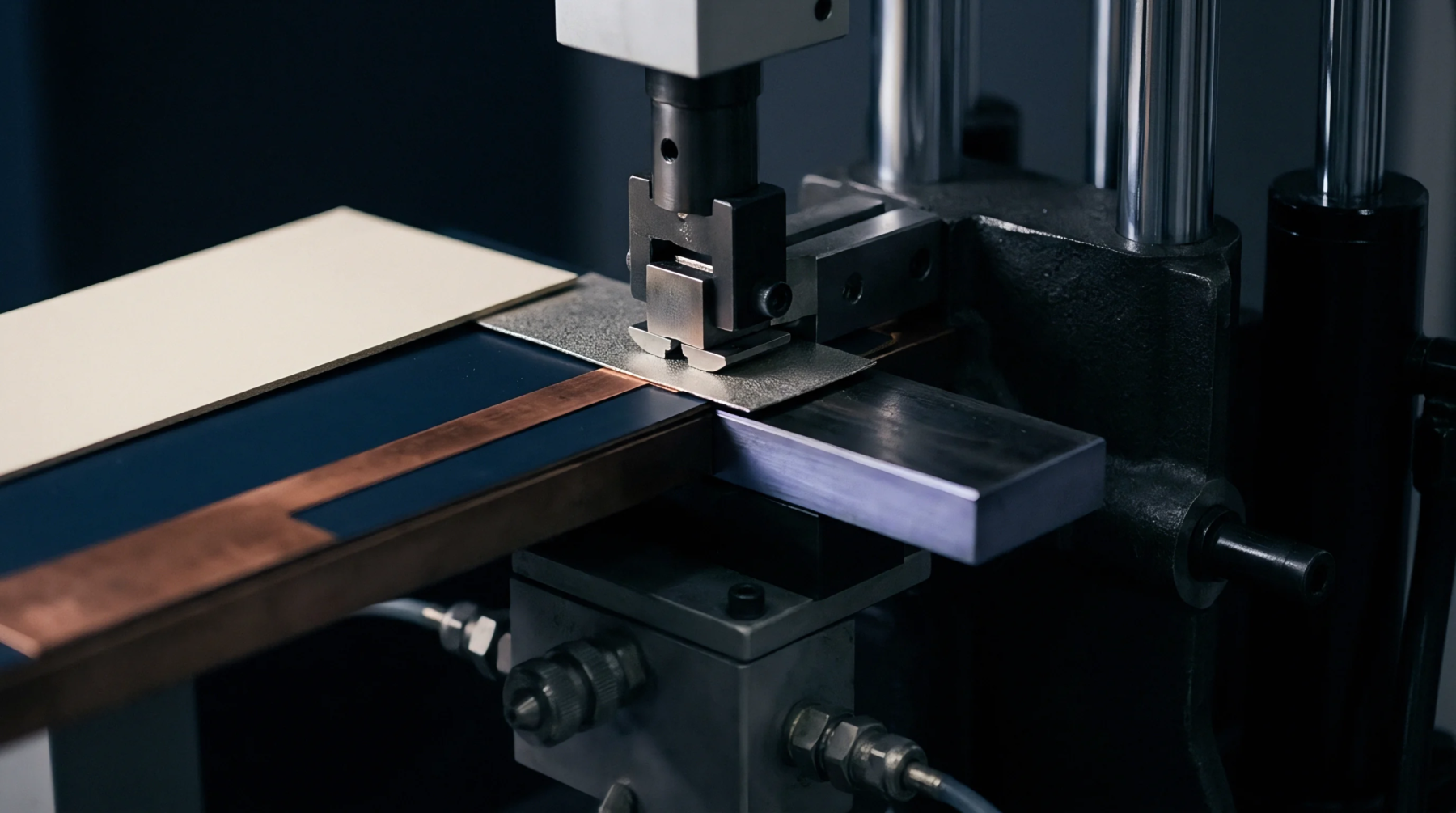
Bonding between the smooth metal and the resin system is achieved through chemical treatments rather than aggressive mechanical teeth. While hvlp copper foil offers superior electrical performance, it requires careful handling during fabrication to prevent delamination. The peel strength is generally lower than that of standard reverse treated foils.
Manufacturers use specialized primers or oxide treatments to ensure the copper adheres to the dielectric during thermal cycling.
Loss Reduction
Insertion loss in high-speed transmission lines is dominated by the roughness of the copper at the dielectric interface. Signals traveling along hvlp copper foil experience less attenuation because the current path is not lengthened by a jagged surface. This leads to cleaner eye diagrams and lower bit error rates in digital communication systems.
The smooth surface also allows for more precise etching of fine-line traces. Designers specify this foil for 5G infrastructure and high-performance computing modules. Reliability is maintained through rigorous testing of the bond integrity.