Printed Circuit Board Differential Trace Impedance Test Methods
Differential trace impedance testing verifies high-speed PCB signal integrity using time-domain reflectometry on panel test coupons.
Differential trace impedance testing verifies high-speed PCB signal integrity using time-domain reflectometry on panel test coupons.
Subtractive etch factor variations along trace runs create localized impedance drift and coherent reflection peaks that severely degrade high frequency return loss.
Vapor phase condensation modeling on heavy copper substrates predicts liquid film thickness to control latent thermal delivery and prevent solder voiding.

Extended thermal shock verification isolates latent perimeter via barrel fractures before high-density printed circuit board batches enter assembly streams.

GHz acoustic attenuation in sub-ten micron dielectric layers limits echo signal-to-noise ratio, requiring picosecond laser acoustics for reliable characterization.

Calculating pressed prepreg thickness requires accounting for copper pattern density, foil height, glass style geometry, and resin flow during cure.
Mitigate differential stripline glass weave skew by combining low-Dk spread glass, multi-ply prepregs, and minimum two-degree routing offsets on drawings.
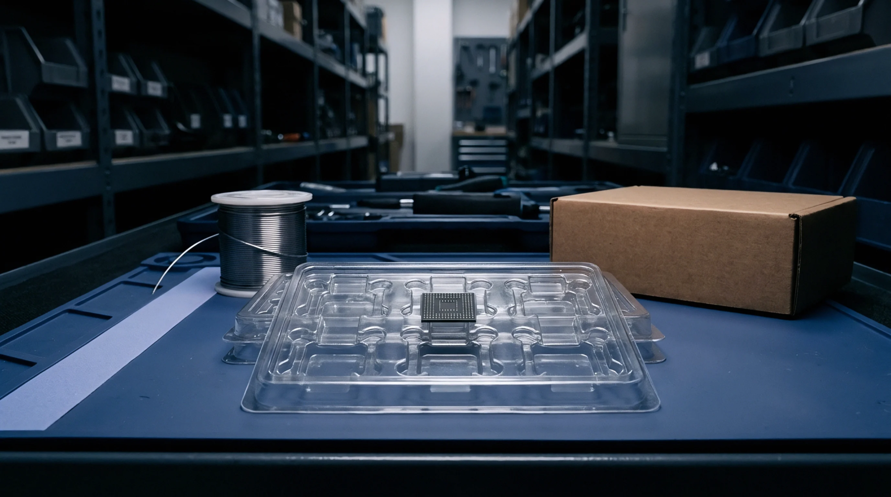
Baseline verification of incoming solder paste requires verifying transit thermal logs, measuring malcom viscosity, and checking powder oxide limits.
High-frequency acoustic phase inversion reveals submicron microvia delamination escaping electrical tests, saving $5.60 per unit over field warranty exposure.

High-frequency acoustic microscopy resolution in multilayer laminates is limited by weave scattering and dielectric attenuation, requiring phased gating.
High temperature viscoelastic relaxation in low-loss dielectrics shifts z-axis strains to microvias, causing interfacial target-pad tears caught only by in-situ testing.
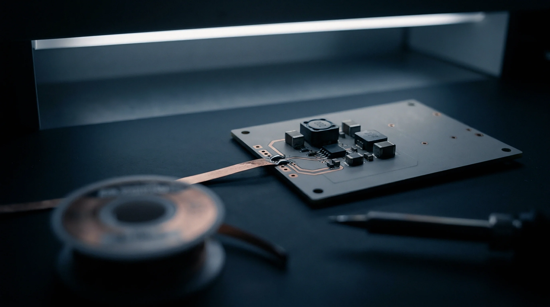
Weibull shape and location parameters derived from microsections quantify true target pad clearance safety margins, protecting buyers from latent dielectric field failures.
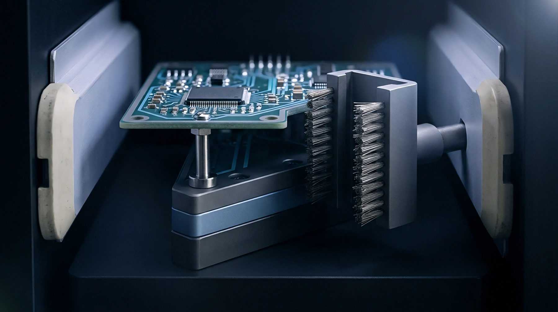
Z-axis laminate expansion exceeding copper ductility during lead-free reflow drives microvia failure, requiring high-Tg filled dielectrics and coupon screening.

Interfacial halogen trapping at electroless nickel interfaces drives thermal embrittlement, requiring ToF-SIMS verification to cap chlorine concentration below critical voiding limits.
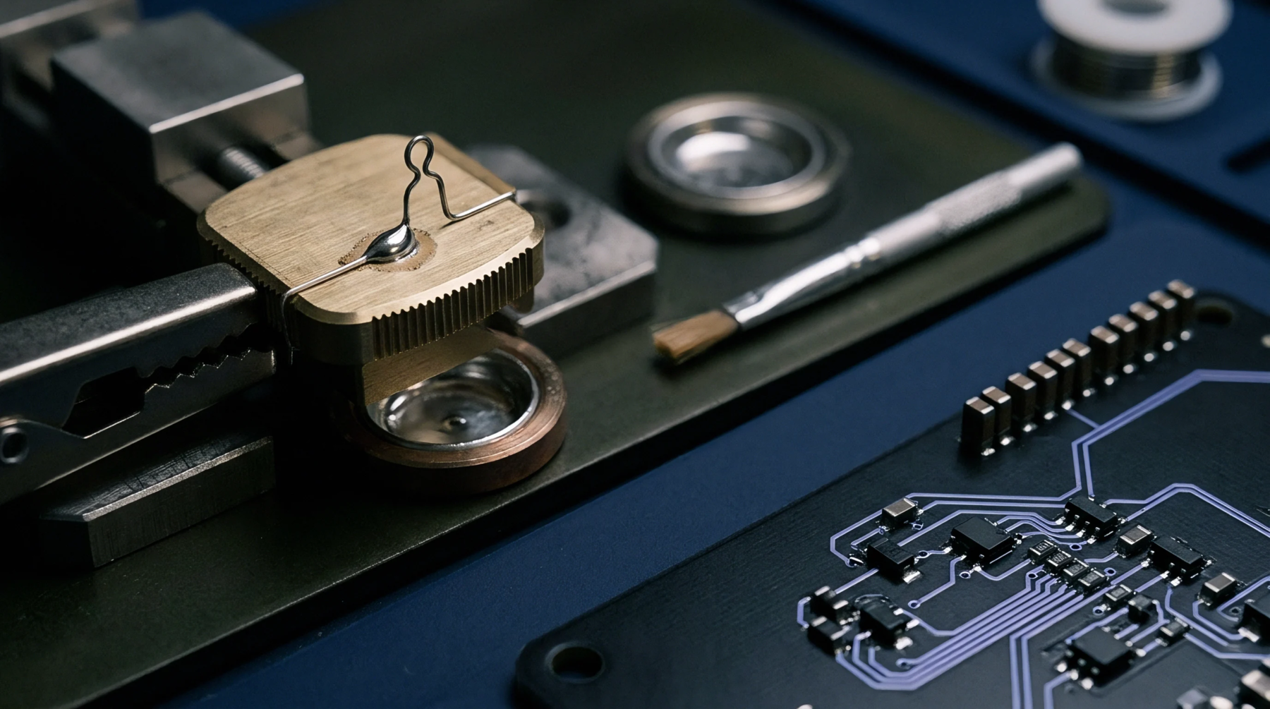
Integrating z-axis dielectric dispersion with resin distribution data prevents impedance mismatches and vertical eye closure in 112G PAM4 channels.
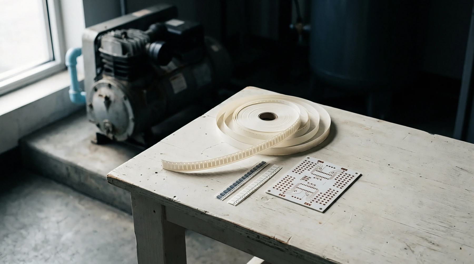
Calculate stripline impedance by applying the geometric mean of in-plane and z-axis permittivity to sidewall fringing fields to eliminate 2-ohm routing offsets.

Resin content mismatch shifts dielectric constants, alters transmission line impedance, and drives thermal warpage unless glass styles and resin volumes balance.
Expertise is a utility, not a secret. sentiention™ publishes its working knowledge as open reference: intelligence layer covering the materials it sources, the markets it enters, and the reference that serves both.