Transmission Topology
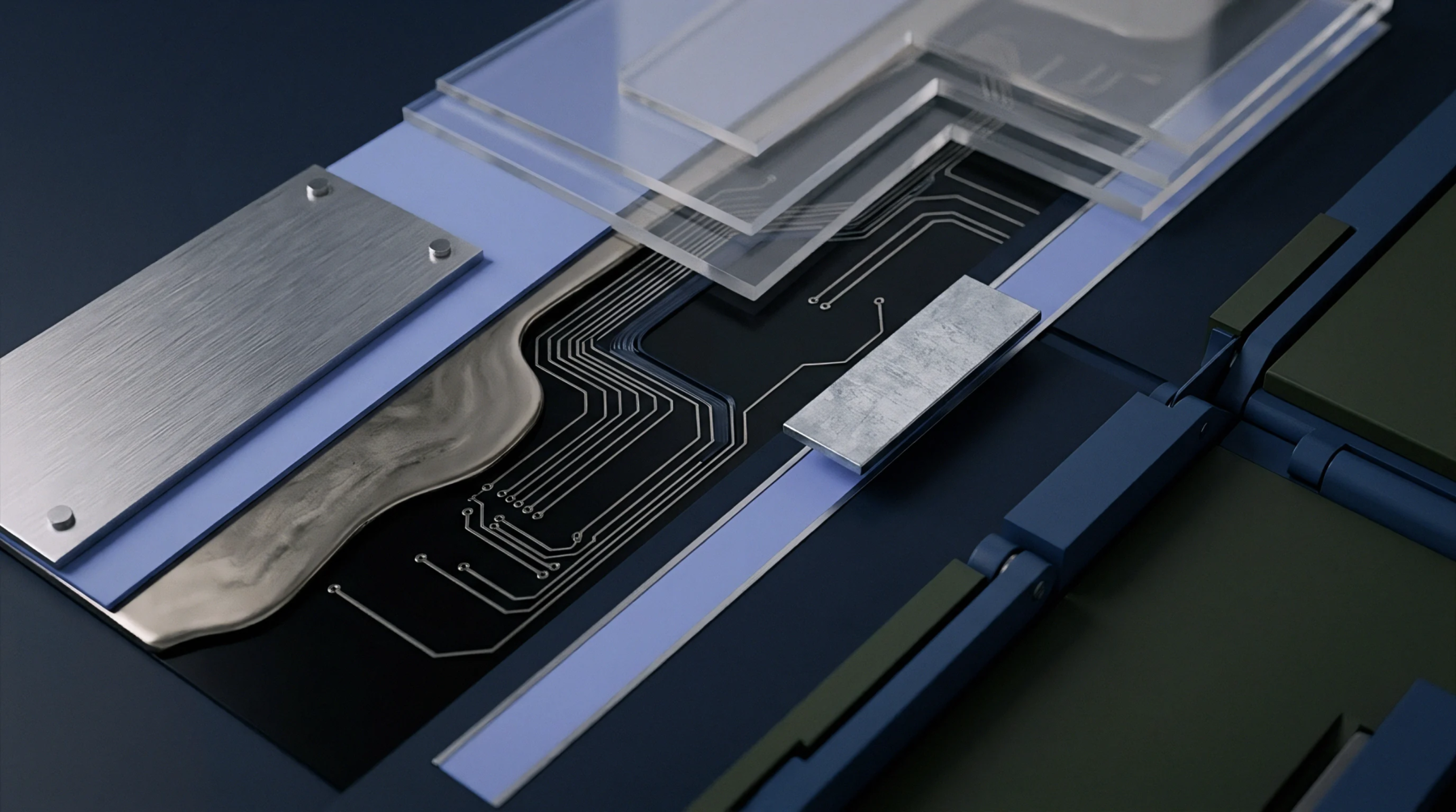
High frequency signaling propagates across a conductive trace separated from a continuous ground plane by a dielectric substrate that maintains a stable electromagnetic field throughout the routing path. Designers utilize microstrip geometry to control impedance and propagation delay in radio frequency circuits. The substrate material determines the velocity of signal movement while the width of the conductor fixes the characteristic impedance.
Manufacturing shops regulate these dimensions through laser direct imaging or chemical etching processes to ensure strict tolerance adherence. Laminate thickness variability introduces phase shifts and signal degradation at higher frequency ranges. Proper copper surface finish selection minimizes skin effect losses.
Manufacturing Variance
Fabrication tolerances influence the finished performance of the interconnection during the etching process. Variations in dielectric constant or copper thickness shift the impedance of a microstrip away from the target value. Inspectors measure the conductor width using automated optical inspection equipment to confirm conformity with design specifications.
Any unintended narrowing of the trace increases inductance and compromises signal integrity. Chemical baths for copper removal require consistent agitation to prevent over-etching or uneven side walls. Operators monitor the etch factor closely to avoid geometry defects that cause reflections.
Controlled impedance testing provides verification that the assembly meets performance requirements before component population. A variation of five percent in dielectric height significantly alters the electrical characteristics of the path. Engineers define allowable limits based on the signal frequency and the tolerable insertion loss for the application.
Impedance Regulation
Effective circuit behavior relies on the precise relationship between the conductor dimensions and the properties of the underlying dielectric material. Maintaining a constant distance between the signal layer and the ground plane prevents electromagnetic interference between adjacent traces. Assembly teams confirm this geometry through time domain reflectometry to isolate discontinuities in the signal chain.
High speed digital systems require these structured paths to manage crosstalk and electromagnetic radiation. Deviations in the reference plane continuity disrupt the return current path and increase noise. Correct board construction ensures that the signal travels with minimal distortion across the length of the interconnect.
The reliability of signal propagation depends entirely on the accuracy of the physical geometry.