Selecting Laminate Materials for High Density Interconnect Stackups
HDI laminate selection balances resin z-CTE expansion, low-Dk glass weave style, and HVLP copper roughness against sequential lamination panel yields.
HDI laminate selection balances resin z-CTE expansion, low-Dk glass weave style, and HVLP copper roughness against sequential lamination panel yields.
Dense smooth foil stackups require synchronized vacuum press cycles and high-resin fine-glass prepregs to prevent micro-cavity voids and dielectric starvation.
Non-linear silane interphase hydrolysis inside substrate micro-cracks degrades high-frequency signal integrity by driving localized dielectric permittivity shifts.
Quantify anisotropic permittivity drift by extracting tensor components across environmental chambers to preserve differential impedance and phase margins.
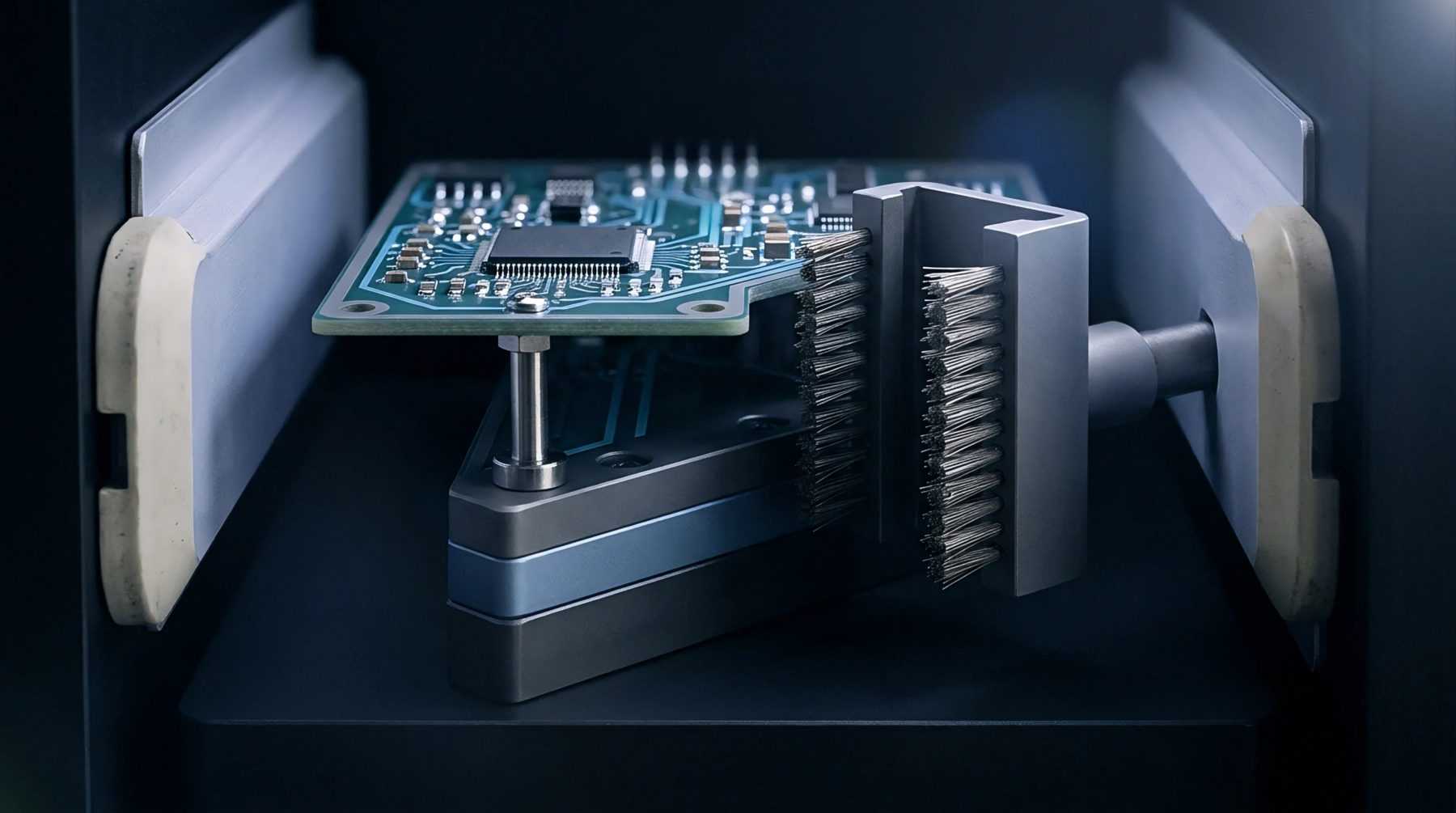
Predictive squeeze flow modeling couples chemorheology and layout copper density to prevent microvia voiding, trace swimming, and dielectric thickness drift.
Managing anisotropic permittivity and glass weave dispersion prevents timing jitter and intra-pair phase skew in gigabit differential interconnects.
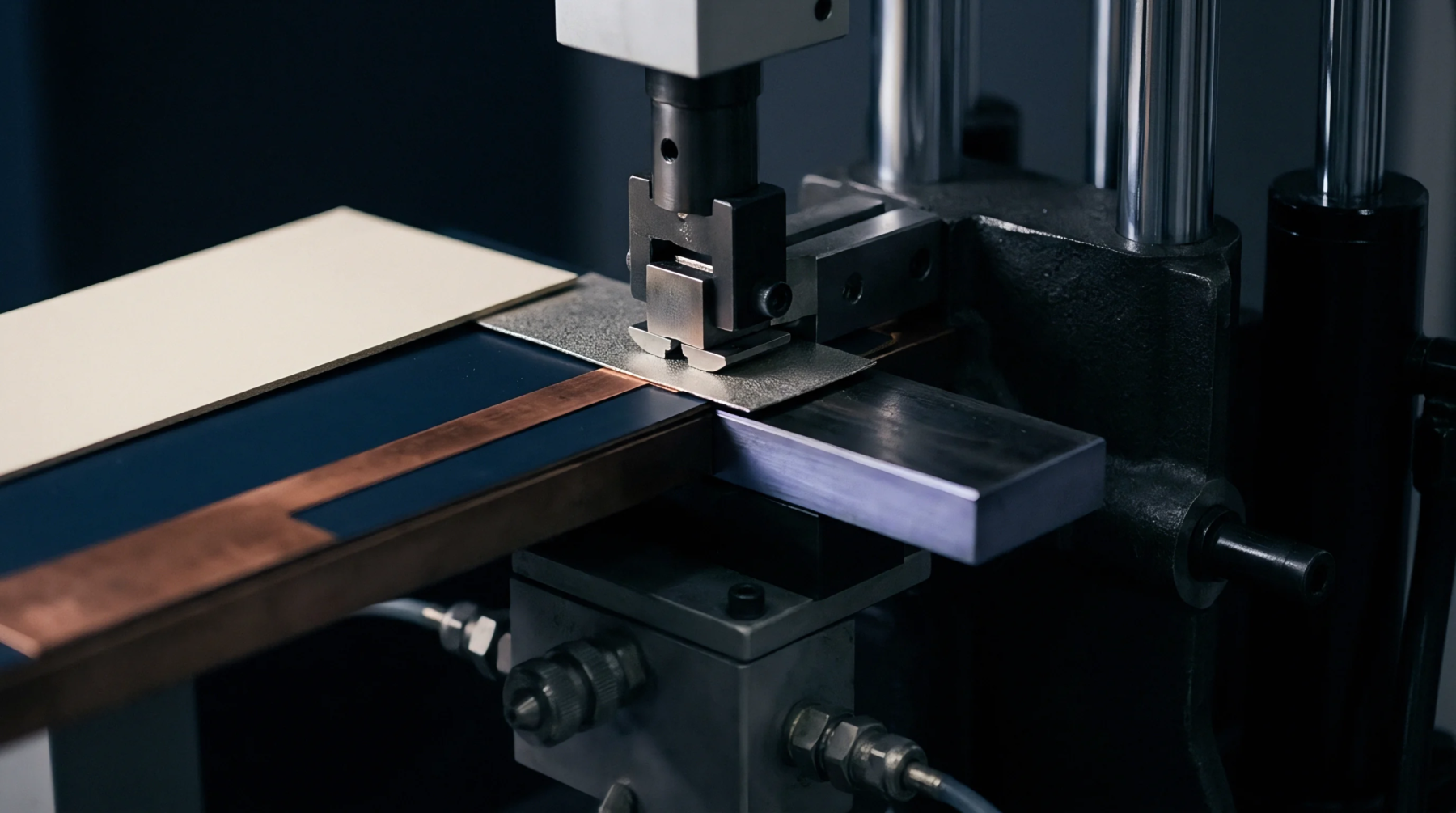
Predict anisotropic sub-core shrinkage by coupling glass yarn orientation with etched copper density across logarithmic decay models for each thermal pass.
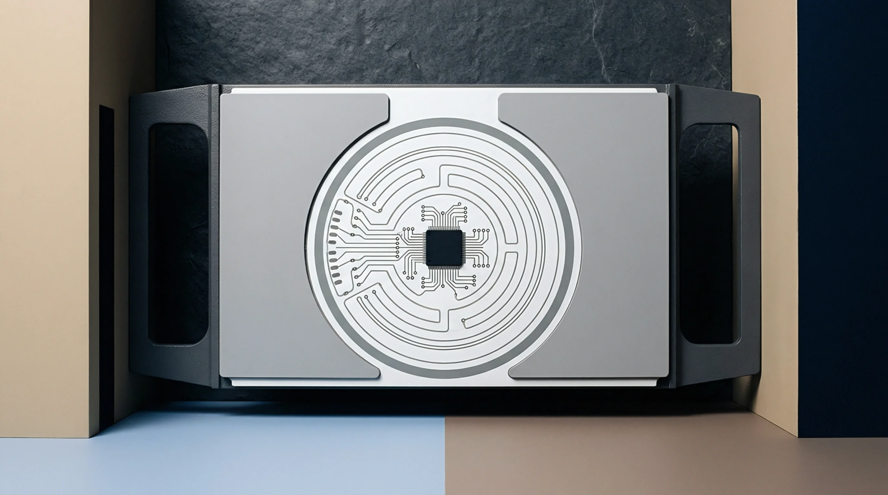
Sequential lamination induces non-linear dielectric relaxation at glass-resin interfaces, shifting Dk up to 0.14 and altering impedance by over 4 ohms.
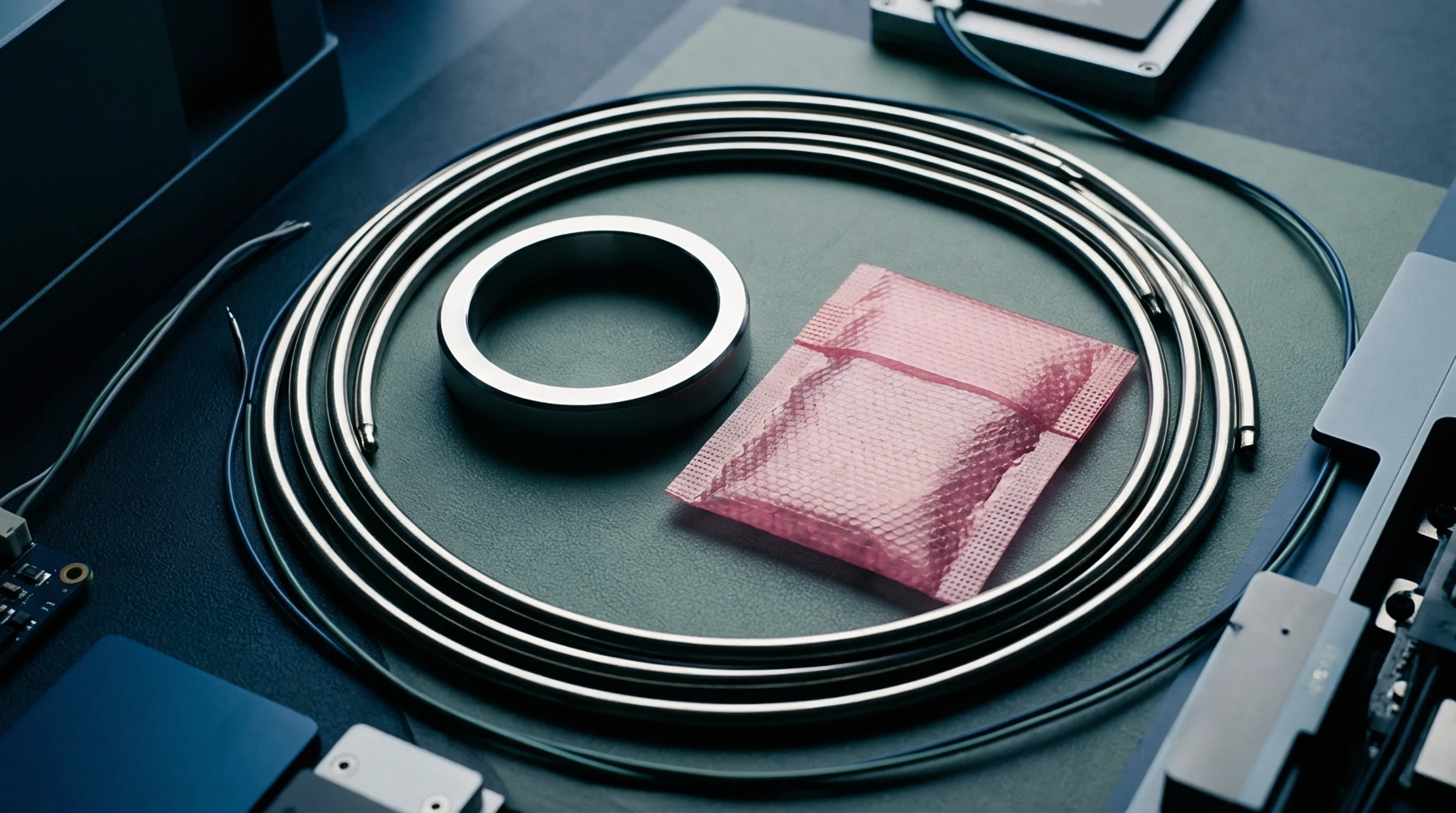
Sub-millimeter spatial dielectric variations from glass weaves and filler distribution shift dynamically under heat, requiring spread glass and low TCDk resins.
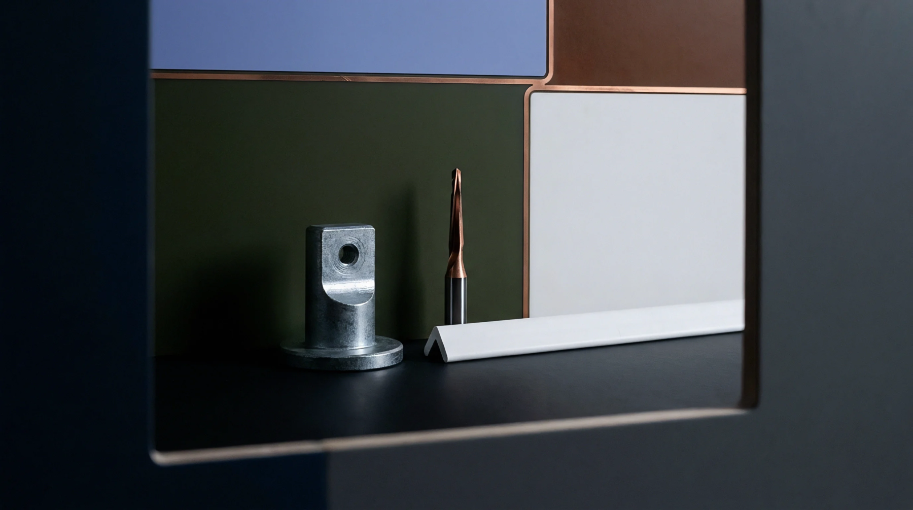
Pairing mid-loss resins with HVLP copper cuts high-frequency trace attenuation by up to 38 percent without forcing transitions to expensive ultra-low-loss substrates.
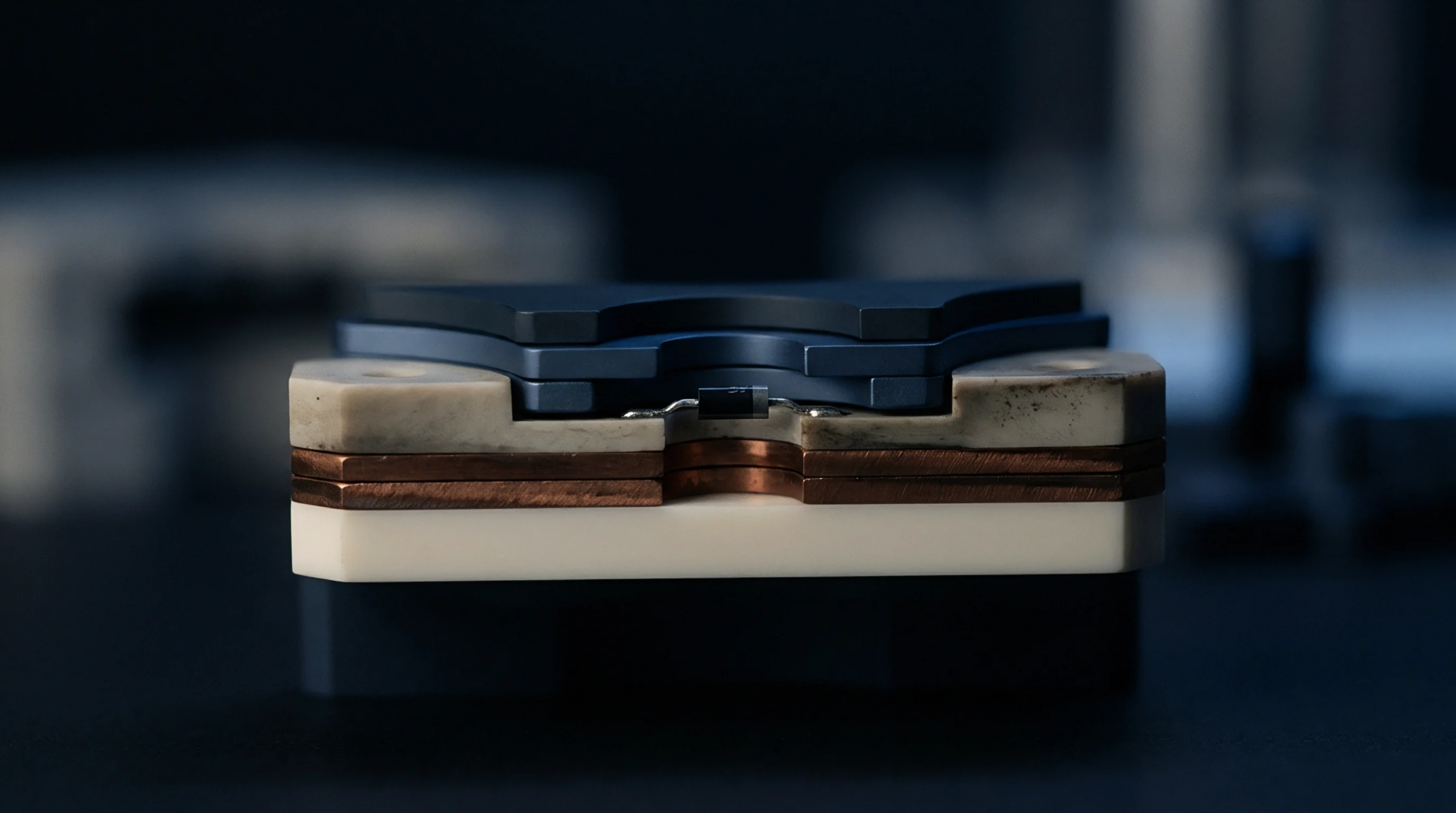
Substrate dielectric drift alters high-frequency signal phase velocity and impedance under thermal stress, requiring flat TCDk resin selection to hold timing margins.
Sequential lamination elevates Z-axis permittivity via resin compaction and thermal cross-linking, requiring pre-compensated CAD trace widths per layer pass count.
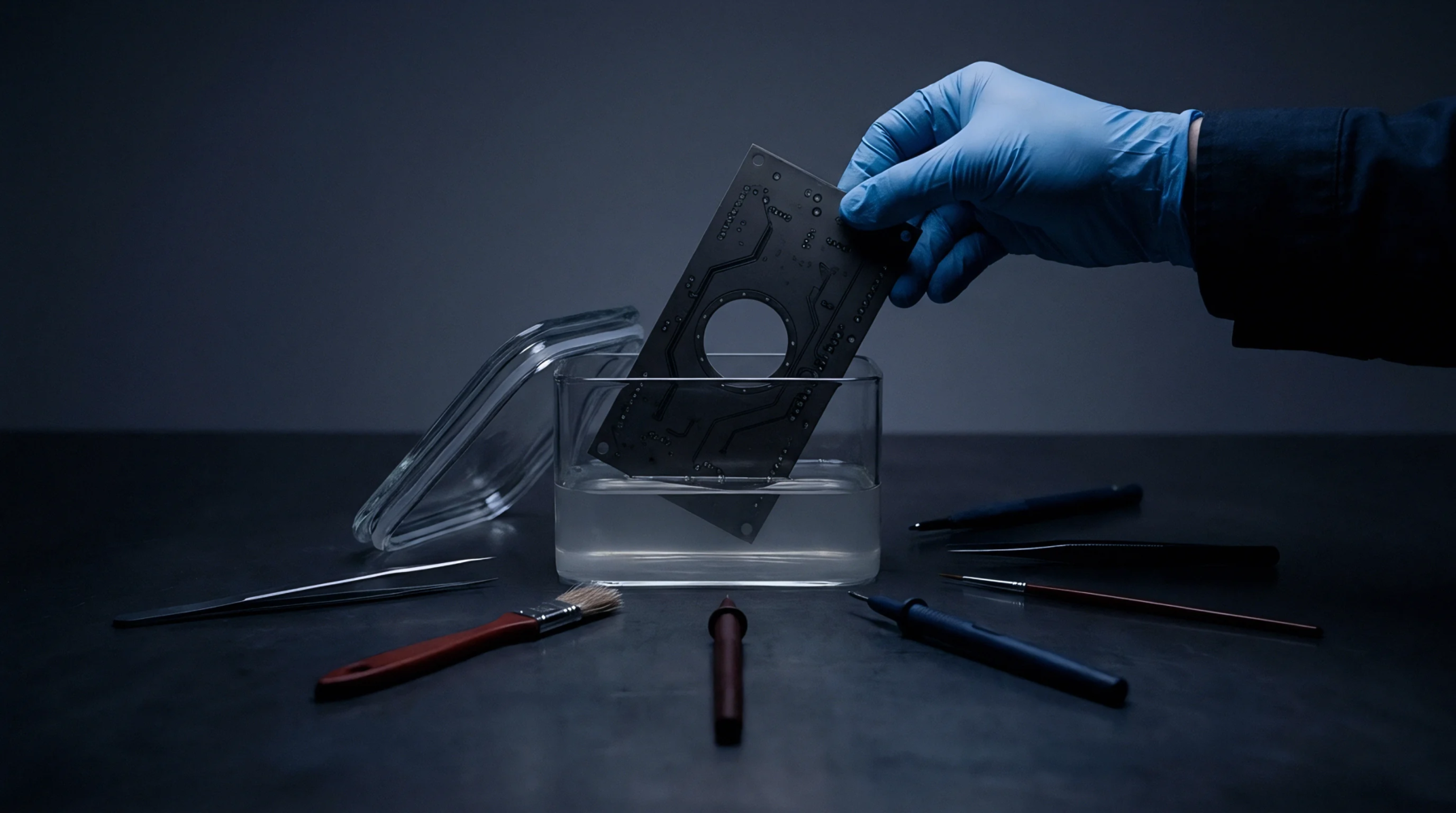
Viscoelastic boundary slip and capillary pressure dictate microvia filling and trace stability during high-density circuit board lamination.
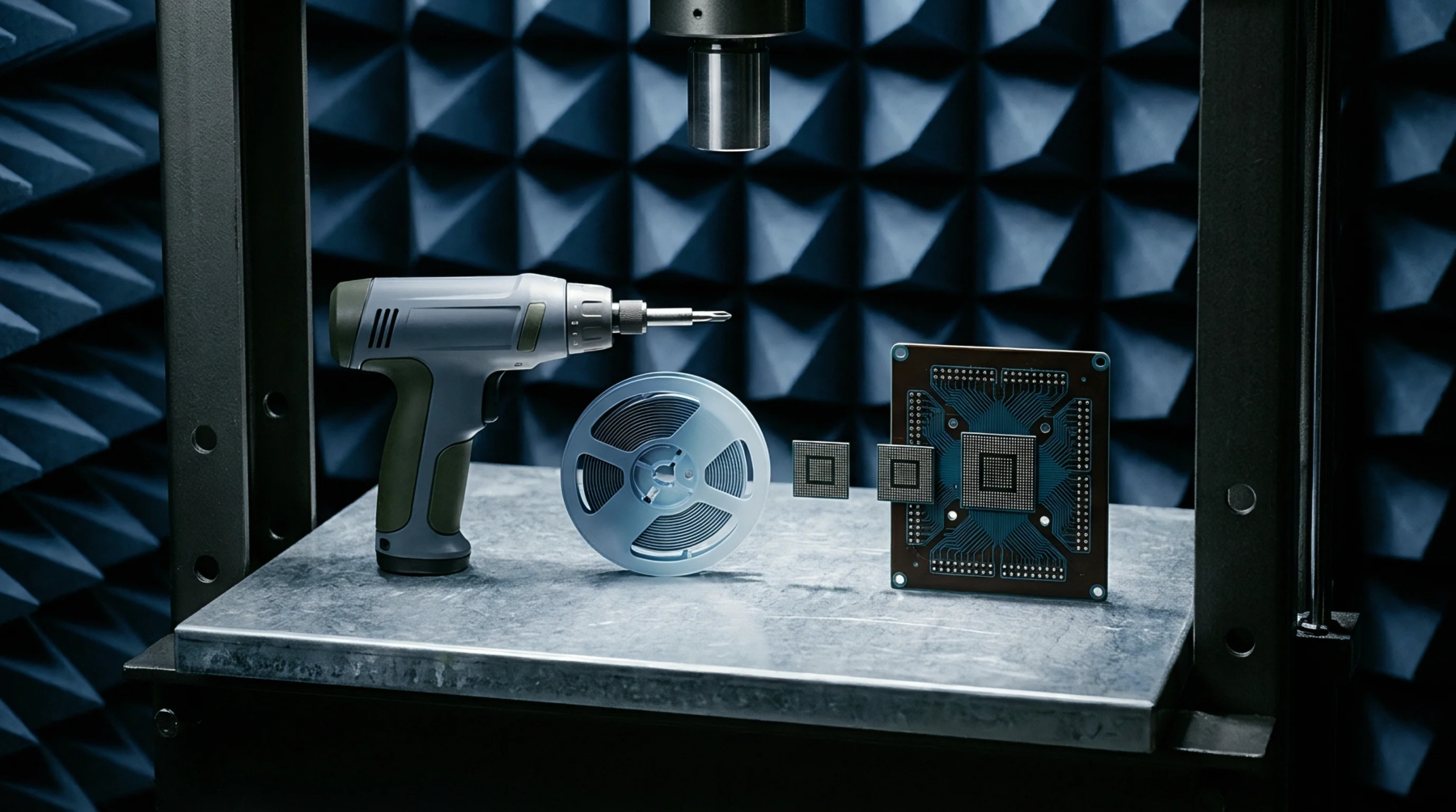
Sub-stack resin squeeze-out during sequential lamination elevates z-axis Dk and reduces dielectric thickness, shifting differential impedance off target.
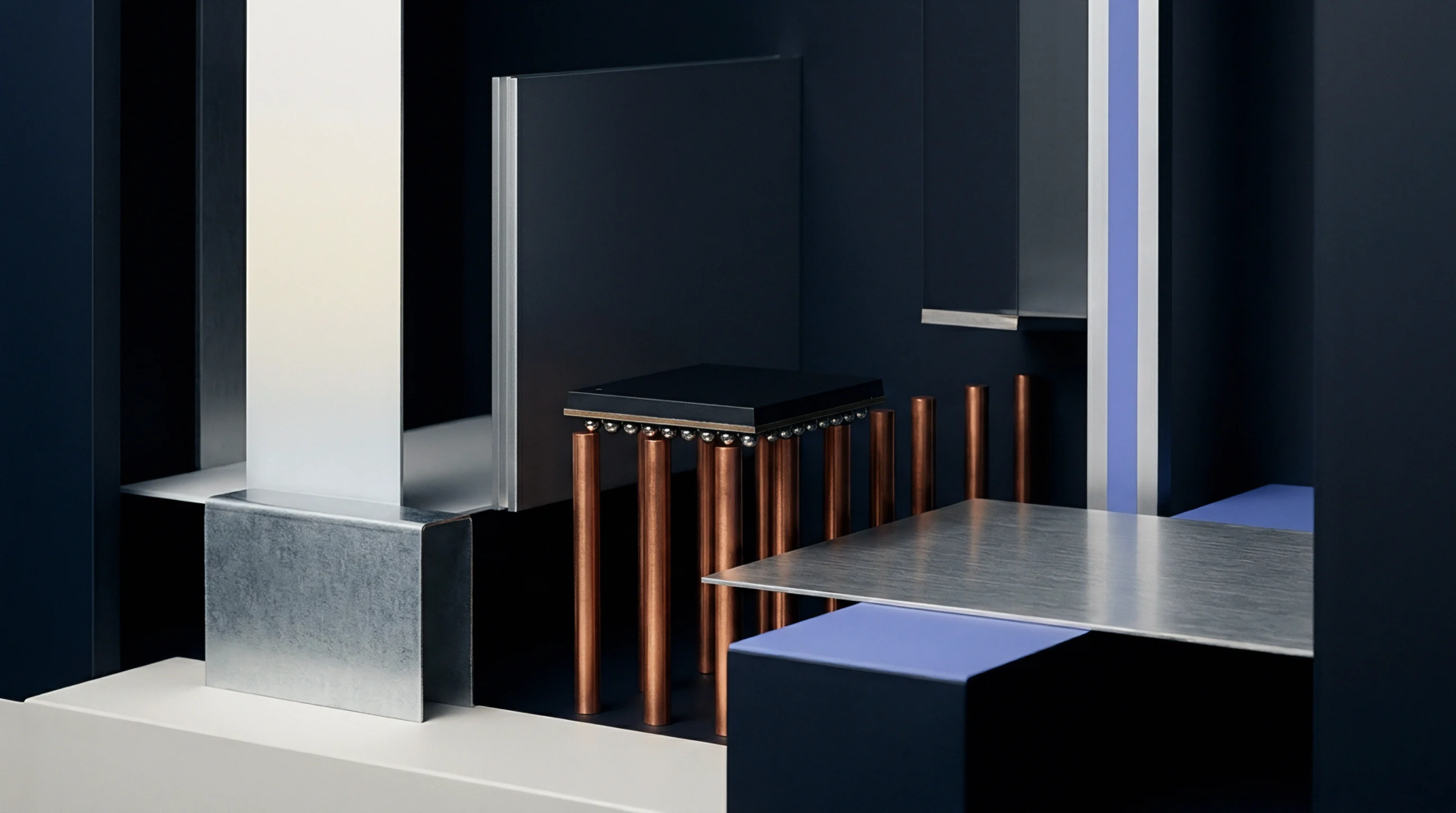
Characterizing spatial dielectric anisotropy under extreme thermal excursions prevents sub-THz phase distortion and catastrophic high-density packaging yield loss.
Expertise is a utility, not a secret. sentiention™ publishes its working knowledge as open reference: intelligence layer covering the materials it sources, the markets it enters, and the reference that serves both.