Quantifying Microstrip Phase Delay Variance Driven by Prepreg Glass Yarn Geometry
Prepreg glass bundle spacing causes local permittivity shifts that introduce picosecond phase delay variance in high-speed microstrip traces.

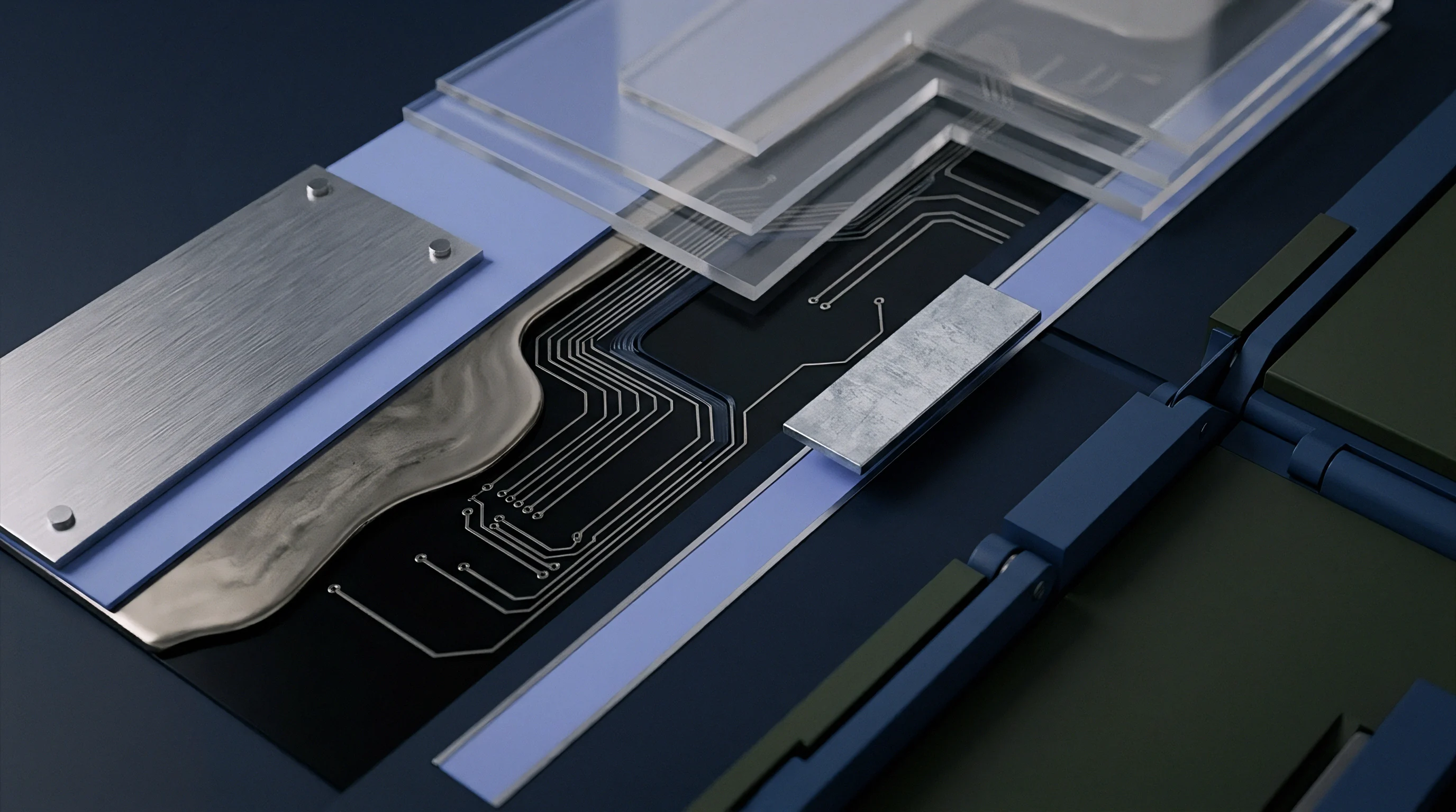
Strand

Filament Topography and Local Permittivity Gradients
Dielectric substrates in high-speed printed circuit boards are composite structures. Standard prepreg layers consist of continuous glass filaments bound into cylindrical yarns and pressed within an epoxy resin matrix. Standard E-glass filaments have a relative dielectric constant (Dk) of 6.1 at 10 GHz, while the surrounding epoxy matrix exhibits a Dk between 3.0 and 3.3 over the same frequency range.
Low-loss formulations (L-glass) reduce filament Dk to roughly 4.6 at 10 GHz, but a spatial mismatch between the glass bundles and resin regions remains. The physical geometry of these glass yarns creates periodic variations in local permittivity across the laminate surface.
Unspread glass styles show marked structural non-uniformity. Style 1080 uses 47 filaments per yarn with a warp pitch of 423 microns and a weft pitch of 423 microns, leaving open resin windows between adjacent yarns. High-frequency microstrip conductors routed directly over these resin pockets encounter an effective local permittivity dominated by the resin Dk. Traces positioned directly over dense yarn intersections experience higher permittivity.
Filament diameter, bundle count, and spreading pressure determine the spatial frequency and amplitude of this dielectric variation.
Resin fills these microscopic gaps.
An unspread yarn cross-section is elliptical or round. Air-jet or mechanical spreading flattens the bundle into a thin, rectangular ribbon. Style 1078 uses the same filament mass as 1080 but flattens the cross-section, reducing the open resin window area from over 15 percent to under 2 percent.
Style 3313 flattens larger bundles to maintain uniform glass distribution across thicker dielectric plies. When spatial gaps between yarns fall below the trace width, the electric field averages across a more uniform medium.
| Glass Style Designation | Filament Diameter (microns) | Yarn Count Warp per Inch | Yarn Count Weft per Inch | Open Window Area (%) | Peak Local Dk Variation (Dk Delta) |
|---|---|---|---|---|---|
| 106 (Unspread) | 5.0 | 56 | 56 | 18.4 | 0.85 |
| 1080 (Standard) | 5.0 | 60 | 60 | 14.2 | 0.72 |
| 1078 (Mechanically Spread) | 5.0 | 60 | 60 | 1.8 | 0.14 |
| 2116 (Standard) | 7.0 | 59 | 57 | 8.5 | 0.58 |
| 3313 (Mechanically Spread) | 6.0 | 60 | 62 | 0.9 | 0.09 |
| 7628 (Standard Heavy) | 9.0 | 44 | 32 | 12.1 | 0.94 |

Micro-Scale Material Inhomogeneity Mechanisms
Local permittivity swings cause impedance shifts and velocity changes along the transmission line. A microstrip trace aligned parallel to an unspread glass bundle incurs a continuous, deterministic phase shift compared to a parallel trace running over open resin. Routing at an angle to the glass weave breaks this continuous shift into periodic phase velocity ripples.
- Resin-rich window alignment lowers effective dielectric constant, accelerating signal propagation speed and reducing line capacitance.
- Glass-bundle center tracking maximizes signal field exposure to high-Dk filaments, slowing phase velocity and increasing delay.
- Periodic bundle crossing induces micro-reflections along the transmission line, raising insertion loss ripple and sub-harmonic phase jitter.
- Differential pair splitting exposes positive and negative signal legs to different dielectric environments, causing intra-pair phase skew.
Laminate suppliers commonly cite bulk dielectric constant measurements taken with split-post dielectric resonators to demonstrate impedance stability. These bulk metrics average properties over several square centimeters, smoothing over micro-scale Dk variations that occur on a 400-micron pitch. Standard documentation accompanying prepreg shipments certifies IPC-4101 compliance, which leaves managing yarn-geometry phase delay variance to the stackup designer.

Propagation
Electromagnetic Phase Velocity Dynamics
Signal velocity along a microstrip trace depends directly on the effective relative permittivity of the surrounding medium. Phase delay per unit length (picoseconds per inch) equals the square root of effective relative permittivity divided by the speed of light in vacuum. In microstrip geometries, field distribution is asymmetric: part of the electric field extends into the air above the trace, while the rest passes through the underlying substrate.
Phase velocity shifts along the trace.
Fringing fields at conductor edges make microstrip phase delay sensitive to top-layer glass yarn placement. Unlike striplines, which sit between symmetric dielectrics, microstrip conductors concentrate a significant portion of total electric field energy in the top 15 to 25 microns of the prepreg. When resin pockets recur periodically along the trace path, effective local permittivity fluctuates with location across the panel.
10 GHz microstrip phase delay varies by up to 2.8 picoseconds per inch when trace trajectory runs parallel to non-spread 1080 glass bundles.
Frequency-Dependent Phase Distortion and Dispersion
At low frequencies, phase delay variance produces little absolute timing shift because signal wavelengths are much larger than the glass yarn pitch. Above 10 gigabits per second ~ where quarter-wavelengths approach the spatial period of the weave ~ phase delay variations turn into inter-symbol interference and duty-cycle distortion. This high-frequency phase delay accumulates over trace length and closes eye diagrams in high-speed links.
Unspread glass styles leave open resin windows.
Total link timing margin depends directly on the trace length over which phase delay accumulates. A 50-ohm microstrip trace on standard 1080 E-glass prepreg (nominal Dk 4.1) has a baseline phase delay around 170 picoseconds per inch. If local Dk ranges between 3.6 and 4.3 due to bundle alignment, phase delay swings between 160 and 174 picoseconds per inch.
Over a 10-inch run, this introduces up to 140 picoseconds of uncompensated phase skew, exceeding the entire unit interval budget of a 28 GHz SERDES receiver.
Ignoring local dielectric fluctuations during microstrip routing risks differential skew, eye collapse, higher bit-error rates, and complete link failure.


Routing
Layout Mitigation Strategies for Yarn Inhomogeneity
Preventing weave-induced phase delay variance requires disrupting the alignment between microstrip traces and glass yarn axes. Standard PCB CAD tools orient traces parallel or perpendicular to panel borders, which mirrors the orthogonal weave of warp and weft yarns. Routing microstrip traces at a slight angle to the grid forces conductors to cross glass bundles and resin windows repeatedly over short distances.
Layout teams apply off-axis routing in two ways: board-level zig-zag paths or panel-level artwork rotation. Zig-zag routing breaks up straight trace runs with periodic diagonal segments. Artwork rotation rotates the entire board pattern relative to raw laminate panel edges during photolithography, angling all straight traces relative to the underlying glass yarns.
Selecting spread glass fabrics with high resin fill factors minimizes localized dielectric contrast across high-speed signal corridors.

Are Diagonal Routing Angles Economical across Multilayer Panels?
Rotating artwork by 5 to 10 degrees relative to the lamination panel breaks yarn alignment across all signal layers simultaneously. However, panel-level rotation increases scrap and yields fewer usable boards from a standard 18-by-24-inch panel. Depending on board geometry, losing usable area adds between 12 and 22 percent to total panel cost.
Designers offset traces by ten degrees.
Zig-zag routing avoids panel scrap by embedding small routing angles directly in CAD layout files. Typical offset angles range from 7 to 11 degrees, with repeat steps matched to the weave pitch. Stepping traces 3 to 5 trace widths over a 500-micron length ensures integration across at least one full warp and weft cycle.
- Determine the warp and weft yarn spatial pitch of the selected laminate prepreg glass style from the manufacturer’s physical construction sheet.
- Calculate the minimum diagonal offset segment length needed to cross at least two complete glass bundle periods based on the yarn pitch.
- Set the trace routing angle between 7 degrees and 10 degrees relative to the primary board edge inside the CAD software constraint manager.
- Apply the diagonal routing constraint to all high-speed differential pairs and critical single-ended clock lines on microstrip outer layers.
- Verify clearance rule compliance along zig-zag segments to prevent trace-to-trace crosstalk violations caused by diagonal steps.
Does the fabrication shop retain sufficient registration margin when microstrip traces are routed diagonally across large-format array panels?


Tolerance
Statistical Phase Delay Modeling and Monte Carlo Analysis
Quantifying microstrip phase delay variance relies on statistical modeling of trace placement relative to yarn pitch. Monte Carlo simulations treat trace offset as a uniform random variable across the spatial period of the weave. For a 100-micron trace on 1080 glass (423-micron pitch), effective glass and resin coverage varies based on lateral trace position.
Tight phase tolerances demand spread glass styles.
Effective dielectric constant is calculated by integrating spatial Dk weighted by electric field energy density. Field intensity peaks directly beneath the conductor and drops off sharply with lateral distance. Consequently, narrow microstrip traces experience larger Dk variations than wide traces because they cover a smaller cross-section of the substrate weave.
| Glass Style & Conductor Topology | Trace Width (microns) | Nominal Dk | Dk Variance Range (Peak-to-Peak) | Phase Delay Variance at 10 GHz (ps/inch) | Max Intra-Pair Skew over 5 Inches (ps) |
|---|---|---|---|---|---|
| 106 Standard Single-Ended | 75 | 4.05 | 0.62 | 2.45 | 12.25 |
| 1080 Standard Differential Pair | 100 | 4.10 | 0.54 | 2.10 | 10.50 |
| 1078 Mechanically Spread Diff Pair | 100 | 4.12 | 0.11 | 0.42 | 2.10 |
| 2116 Standard Differential Pair | 125 | 4.25 | 0.38 | 1.48 | 7.40 |
| 3313 Mechanically Spread Diff Pair | 125 | 4.28 | 0.07 | 0.28 | 1.40 |
| 7628 Heavy Glass Differential Pair | 200 | 4.40 | 0.48 | 1.85 | 9.25 |

Copper Foil Roughness and Dielectric Thickness Interplay
Glass weave is not the only source of phase delay variation; electrodeposited copper foil profiles also contribute directly. Surface roughness slows signal propagation by lengthening the electrical path along the copper-dielectric interface. Standard rolled or low-profile electrodeposited copper has peak-to-valley profile heights (Rz) between 3.0 and 6.0 microns, while Very Low Profile (VLP) and Hyper Low Profile (HVLP) coppers maintain Rz below 1.5 microns.
Copper foil roughness shifts phase velocity further.
Variations in dielectric thickness from prepreg resin flow compound weave-induced shifts. Lamination press pressure forces resin into copper clearance voids on adjacent inner layers, altering local prepreg height by up to 10 percent. A local drop in dielectric thickness raises line capacitance and effective permittivity, shifting phase delay in the same direction as a high-Dk glass bundle.
IPC-4101 slash sheet declarations omit weave pitch uniformity, shifting structural skew responsibility entirely onto fabrication stackup notes.
To manage phase delay variance in production, engineering procurement documentation must specify explicit stackup and material rules prior to RFQ release.
- Spread glass qualification notes require fabricators to supply mechanically flattened prepreg styles for all microstrip outer-layer dielectrics.
- Low-profile copper foil specifications mandate HVLP or VLP copper foils on microstrip layers to decouple surface roughness phase delay from yarn variations.
- Pressed thickness tolerance limits restrict post-lamination dielectric height variance to within plus or minus 5 percent of nominal stackup targets.
- Coupon-based TDR skew verification obligates the fabricator to include phase delay test coupons on all production panel borders.
Sizing microstrip trace widths to at least twice the yarn pitch helps average out spatial Dk variations across the dielectric.

Loom
Mechanical Yarn Spreading Technology and Fabric Standard Limits
Mechanically spread prepregs are produced by passing glass strands through high-pressure water jets, air knives, or tension rollers before resin impregnation. This flattens individual filaments across warp and weft axes, closing resin gaps. Spread styles like 1035, 1078, and 3313 provide consistent structural dielectric performance across the prepreg sheet.
Mechanical spreading flattens the glass bundles.
Standard industry specifications do not cover micro-scale dielectric variations. IPC-4101 slash sheets focus on macro-level electrical, thermal, and chemical properties. Standard test methods under IPC-TM-650, such as clamp-cavity and split-post resonator tests, measure dielectric constant averaged over areas larger than several square inches.
As a result, prepreg that fully complies with IPC-4101 parameters can still show local Dk fluctuations large enough to exceed high-speed differential skew budgets.
Trace widths exceeding two yarn repeat periods integrate localized permittivity variations into an averaged bulk phase delay.
Procurement Dossier Specifications for Phase-Critical Stackups
Procurement documentation must explicitly name glass styles to keep fabricators from substituting unspread prepregs during factory loading. When fabrication drawings specify only target impedance and dielectric thickness, factories often swap spread 1078 for standard 1080 to reduce material costs. Calling out exact glass styles on engineering drawings prevents these unauthorized substitutions.
Standard slash sheets omit bundle pitch specs.
Fabrication notes for phase-critical boards need clear execution rules. Drawings should state allowed prepreg glass styles, minimum resin percentages, copper foil profile tiers, and coupon test requirements. Without these explicit drawing notes, factories remain free to select any IPC-4101 compliant material that meets nominal impedance targets.
IPC-4101 slash sheet specifications bind laminate suppliers to macro-scale electrical parameters, while leaving localized prepreg yarn geometry variations entirely unconstrained unless custom fabrication drawing notes are appended.
Cost

Commercial Impact of Material Selection and Array Yield
Specifying spread glass and low-loss laminate systems increases raw board costs. Standard E-glass 1080 prepreg provides a baseline cost for multilayer high-speed stackups. Mechanically spread prepregs add a 15 to 30 percent material premium due to additional loom processing and tighter spreading quality controls.
Laminate press pressure alters dielectric thickness.
Combining low-loss L-glass with mechanically spread yarns raises costs further, increasing prepreg square-meter pricing by 45 to 70 percent over standard E-glass. Foil upgrades add another layer: moving from standard electrodeposited copper to HVLP foil increases total copper sheet costs on the panel by 8 to 14 percent. Still, these raw material adders are modest compared to yield losses at final functional testing.
| Prepreg Construction & Foil Combination | Relative Material Cost per Square Metre | Panel Yield at 10 GHz (5 ps Skew Limit) | Panel Yield at 28 GHz (2 ps Skew Limit) | Estimated Unit Board Cost Delta (%) |
|---|---|---|---|---|
| Standard E-Glass 1080 + ED Copper | 1.00 | 82% | 41% | Baseline |
| Mechanically Spread E-Glass 1078 + ED Copper | 1.22 | 98% | 84% | +8% |
| Mechanically Spread E-Glass 1078 + HVLP Copper | 1.34 | 99% | 95% | +14% |
| Spread L-Glass 1078 + HVLP Copper | 1.62 | 100% | 99% | +26% |
| Spread L-Glass 3313 + HVLP Copper | 1.58 | 100% | 98% | +23% |
Panel Utilization and Factory Qualification Bounds
Panel yield dictates true unit cost.
Rotating artwork to avoid yarn alignment reduces panel utilization. Angling board outlines by 10 degrees on an 18-by-24-inch lamination panel typically reduces board count per panel by 15 to 25 percent. Because bare-board pricing is assessed per processed panel rather than per board, lost area directly raises unit costs.
For high-speed designs operating above 25 gigabits per second, combining mechanically spread prepregs with standard straight routing delivers the best commercial yield ~ avoiding panel scrap while keeping phase delay variance within timing budgets. Partnering with qualified lamination facilities that control prepreg yarn alignment to tight angular tolerances ensures repeatable phase delay performance in volume production.