Electrochemical Deposition Process
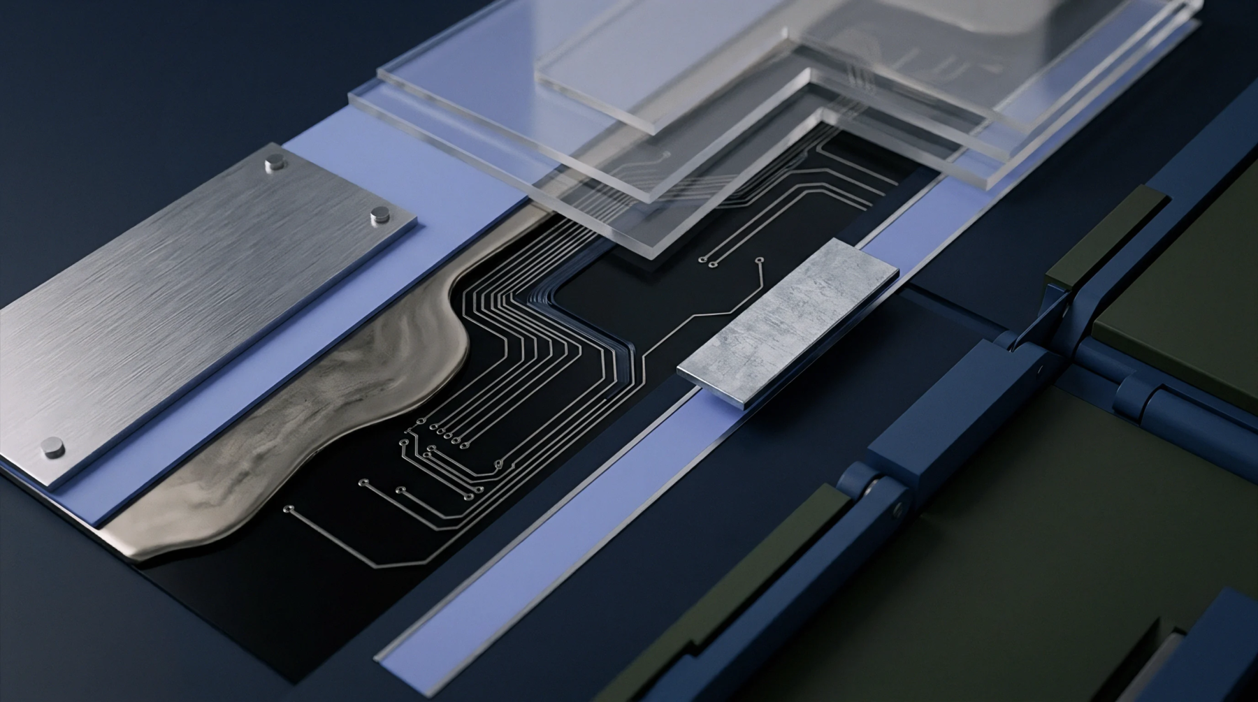
Electrolytic metal buildup provides the conductive pathways within printed circuit boards through the reduction of copper ions from a liquid solution onto a prepared substrate surface via an externally applied current. Such electrodeposited copper requires a highly controlled bath chemistry to ensure that the deposited metal achieves the uniform grain structure necessary for thermal reliability. Additives within the electrolyte govern the rate of ion migration at high current densities to prevent the formation of dendritic growths or voids.
Mechanical properties of the metal depend upon the ratio of acid to metal ions and the presence of organic brighteners that influence the final grain size. Adhesion to the underlying conductive foil rests upon the surface topology created during the initial seed layer application. Current distribution patterns determine the thickness of the plating in complex geometries such as blind vias or high aspect ratio through holes.
Plating Integrity Metric
High tensile strength remains the primary requirement for copper deposited inside narrow barrel apertures where expansion forces during thermal cycling exert significant stress. Testing laboratories measure the ductility of the electrodeposited copper by subjecting a test coupon to controlled stretching until failure occurs. Laminate voids or contaminants within the electrolyte often initiate crack propagation during reflow or subsequent operational exposure to rapid temperature shifts.
Microsection analysis confirms that the deposited layers lack laminations or excessive porosity that might weaken the interconnect. Chemical composition limits for trace contaminants prevent the metal from becoming brittle or overly susceptible to oxidative corrosion over the long term.
Manufacturing Boundary Condition
Uniform coverage across the entire panel surface serves as the constraint for plating geometry during final circuit board fabrication. Operators maintain the cathode agitation levels to ensure fresh solution reaches the deepest portions of the circuitry features. Variations in the current flow across the panel surface lead to thicker deposits near the edges and thinner metal within the central areas.
Process engineers calibrate the rectifier outputs to mitigate these edge effects and ensure compliance with IPC standards for finished wall thickness. Proper electrolyte maintenance prevents the accumulation of decomposition byproducts that compromise electrical conductivity. Metallic density within the hole barrel provides the final reliability factor for signal transmission.