Rigid Flex Stackup Selection against Discrete Board Interconnects
Rigid-flex stackup selection replaces failure-prone discrete connectors with continuous polyimide trace runs, trading lower bare-board cost for reliability.
Interface
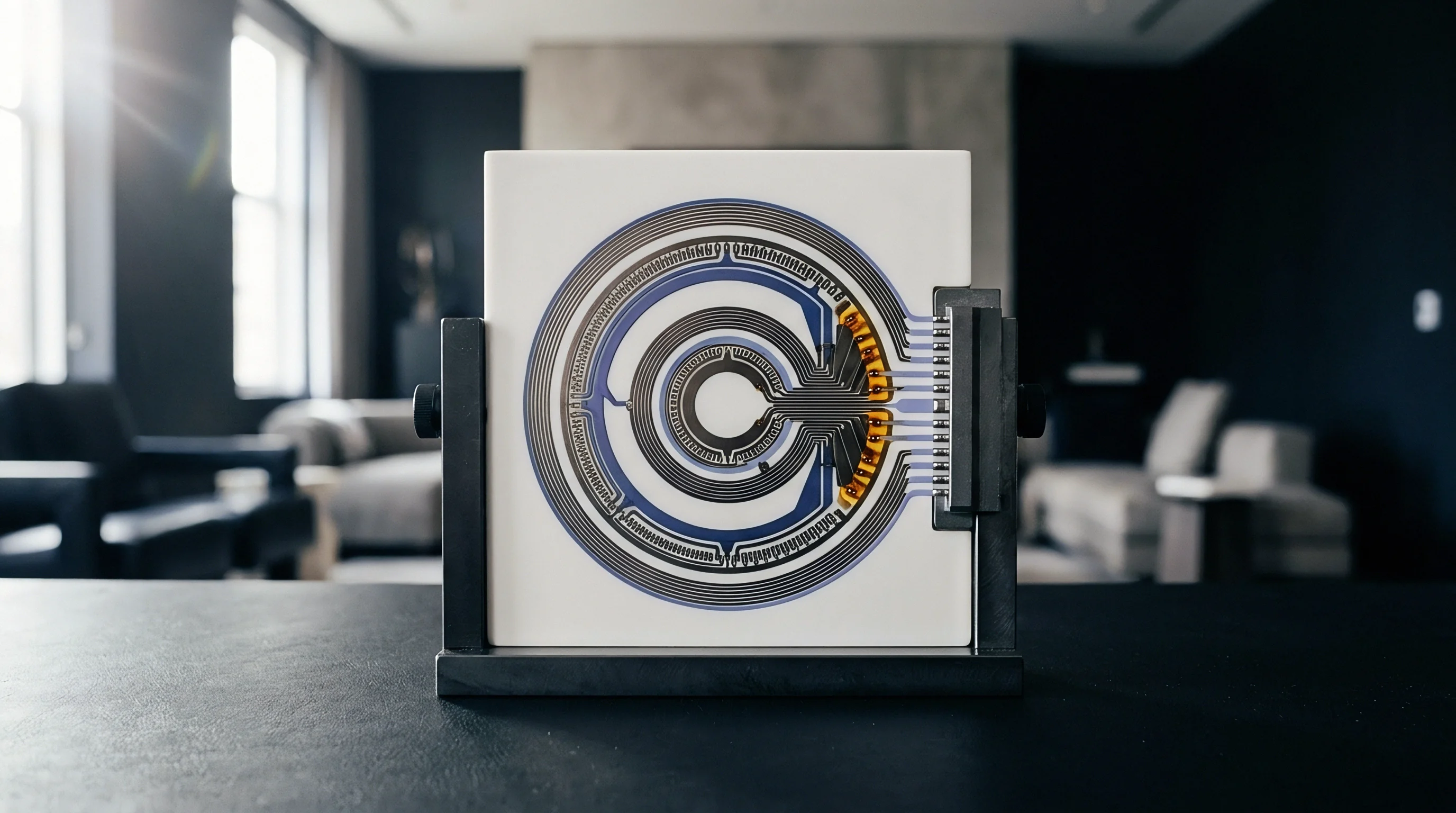
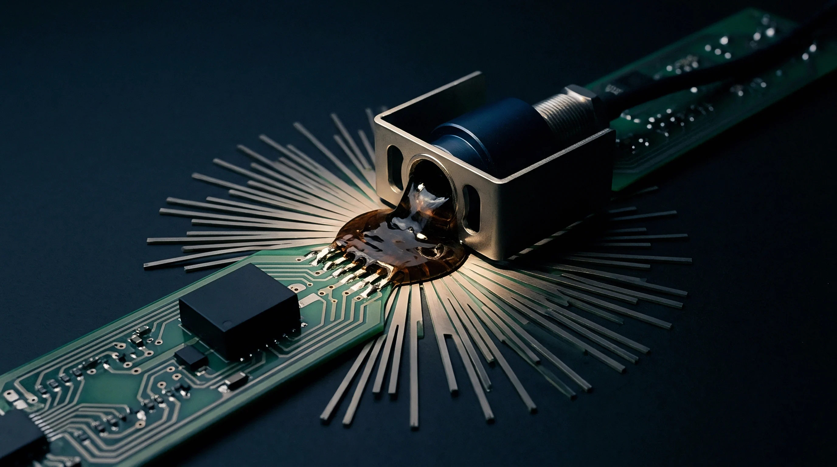
Balancing packaging density against assembly throughput often comes down to comparing bare copper traces in continuous polyimide with discrete connector pins and cabling. Integrated flex structures replace pin-and-socket junctions with continuous copper foil, removing the mechanical interconnects that introduce parasitic inductance and contact resistance. A standard dual-row board-to-board connector adds roughly 1.0 to 1.5 nanohenries of parasitic inductance per contact pin, plus parallel capacitance between adjacent lands.
Running traces straight through flexible dielectric layers maintains a uniform geometric cross-section, preserving characteristic impedance without the physical discontinuities of a connector header.
Abrupt shifts in conductor geometry and reference plane spacing at a connector junction create return loss peaks in high-speed digital or RF channels. While insertion loss through a 50-ohm polyimide flex strip stays smooth up to 28 gigahertz, discrete board-to-board connectors show pronounced S11 reflections above 5 gigahertz unless specialized, high-cost interconnect headers are used. Extending reference ground planes straight through the transition zone in an integrated rigid-flex stackup avoids ground loop inductance and common-mode radiation.
Choosing between an integrated stackup and discrete cabling involves balancing overall enclosure geometry against the assembly workflow. Cable assemblies permit modular sub-assembly testing before final chassis integration, while rigid-flex panels permanently bond every sub-circuit into a single unit during fabrication.
- Quantifying Packaging Envelope Metrics maps available cubic volume inside the enclosure, accounting for required bend radii and clearance around moving mechanisms.
- Evaluating Pin Count Demands tallies all signal, power, and ground nets crossing board boundaries to weigh connector footprint overhead against flex layer counts.
- Mapping Thermal and Motion Vectors separates continuously moving zones from static bends, highlighting strain points where copper can fatigue.
- Simulating Channel Insertion Loss models high-frequency signal integrity across connector land patterns compared to unbroken polyimide microstrip routes.
Architectural Bounds of Integrated Polyimide Linkages
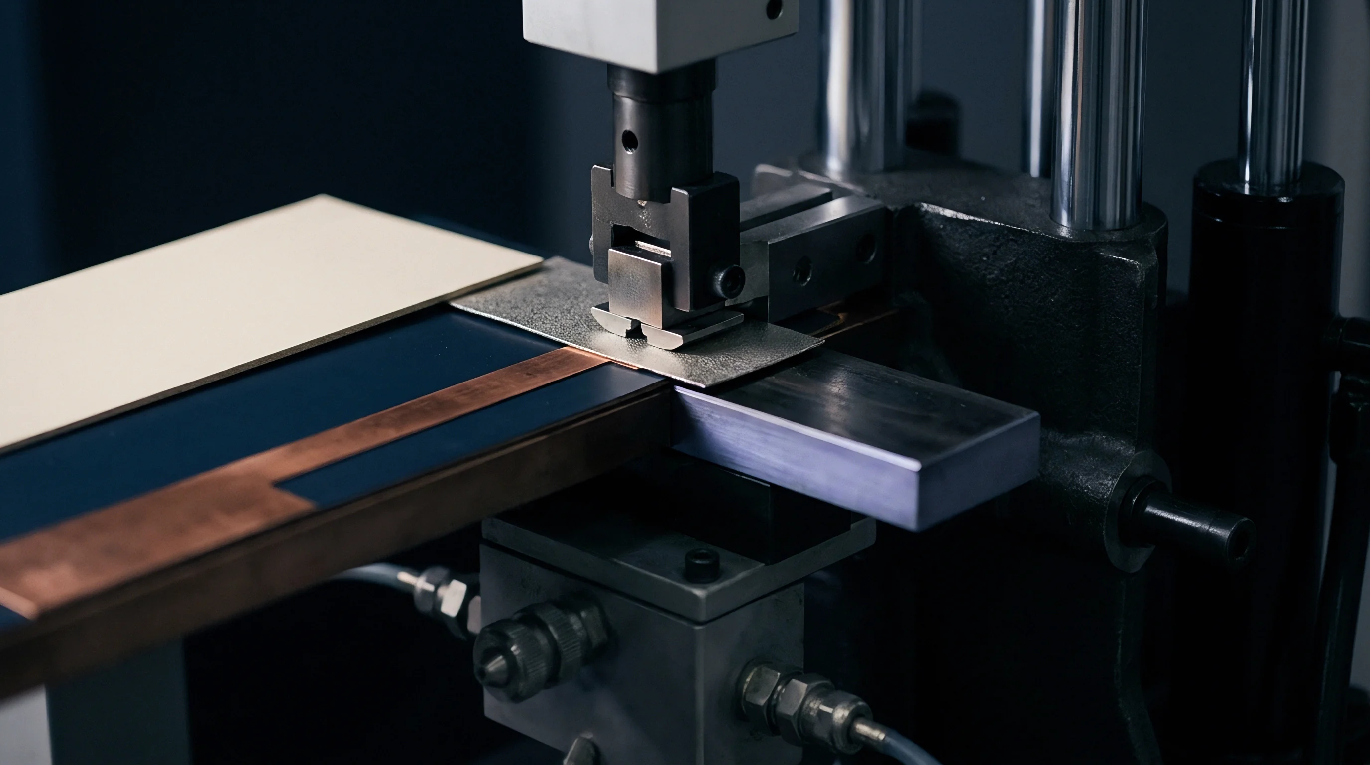
When separate cables connect rigid boards, every board edge requires mechanical termination. Building flexible polyimide cores directly into the primary PCB stackup eliminates surface-mount headers and cuts Z-axis height. A low-profile board-to-board connector pair takes up 1.5 to 4.0 millimeters of vertical height, while a two-layer flexible arm occupies under 0.25 millimeters.
That height savings opens up internal volume for battery cells, heat spreaders, or shielding.
Eliminating mechanical interconnects shifts where assembly risks occur. Discrete cable harnesses require manual insertion or crimped pins, leaving room for unseated contacts, bent pins, or damaged latches. Rigid-flex assemblies arrive at surface-mount lines as a single, fully testable bare board, relying on automated photolithography and laser drilling rather than manual assembly for interconnect accuracy.
Signal Integrity and Discontinuity Mechanics
Transmission line impedance relies on continuous reference planes and uniform dielectric spacing. Discrete wire harnesses and flexible flat cables (FFC) break ground continuity at the connector housing, forcing return currents through designated ground pins. This wider current loop creates localized impedance spikes of 15 to 30 ohms above target, adding measurable jitter to multi-gigabit differential pairs.
Interconnect pin density limits the volumetric efficiency of multi-board enclosures when mechanical shock demands structural latches.
Maintaining reference plane continuity across a rigid-flex junction requires running solid or hatched copper ground shields directly from the rigid board through the flex area. A hatched copper ground plane with a 45-degree grid pattern controls impedance while keeping the arm flexible, avoiding the stiffness of solid copper sheets. Differential pairs routed over 50-percent open hatched ground planes hold impedance tolerances within plus or minus 8 percent across the flex region.
Choosing discrete connectors to save on polyimide tooling often leads to an extra redesign cycle when operational vibration unseats pins in the field.
Foil
Choosing dielectrics for flexible stackups starts with deciding whether acrylic bonding agents can be tolerated in the thermal and electrical path. High-reliability designs specify adhesiveless polyimide laminates, where copper foil is deposited or cast directly onto the polyimide film. Removing acrylic adhesive eliminates the main cause of thermal expansion mismatches and moisture absorption.
The choice of copper foil determines how well the flexible arm handles repeated bending. Rolled Annealed (RA) copper is cold-rolled to stretch its grain structure horizontally along the foil length. This parallel grain orientation lets RA copper survive hundreds of thousands of flex cycles without micro-cracking.
Electrodeposited (ED) copper has a vertical, columnar grain structure that fractures quickly under dynamic stress, making it suitable mainly for static, bend-to-fit applications.
Standard polyimide films absorb up to 1.5 percent water by weight in ambient humidity, compared to less than 0.2 percent for standard FR-4 epoxy laminates. Water trapped in internal layers vaporizes into high-pressure steam during thermal reflow, causing delamination along core interfaces if pre-bake routines are skipped.
Substrate Metallurgical and Dielectric Selection
Polyimide films provide the backbone for flexible stackups, offering high dielectric breakdown strength and flexural durability. Dielectric constants should be checked at actual operating frequencies rather than standard 1-megahertz reference points. Adhesiveless polyimide cores maintain a stable dielectric constant of 3.2 to 3.4 from 1 to 10 gigahertz, with a dissipation factor of 0.003 to 0.005.
Acrylic adhesives push the dielectric constant near 3.6 and dissipation factors above 0.02, increasing high-frequency attenuation.
| Material Configuration | Dielectric Constant (10 GHz) | Dissipation Factor (10 GHz) | Z-Axis CTE (ppm/°C) | Moisture Absorption (%) | Dynamic Flex Endurance |
|---|---|---|---|---|---|
| Adhesiveless Polyimide (RA Copper) | 3.20 | 0.0035 | 16 | 0.80 | Exceeds 100,000 Cycles |
| Adhesiveless Polyimide (ED Copper) | 3.25 | 0.0040 | 18 | 0.85 | Fails Below 10,000 Cycles |
| Acrylic-Bonded Polyimide (RA Copper) | 3.55 | 0.0210 | 110 | 2.80 | Moderate Endurance |
| High-Tg FR-4 Rigid Core (Reference) | 4.30 | 0.0150 | 45 | 0.15 | Zero Flex Capacity |
Matching copper foil surface roughness to signal loss requires a trade-off at higher speeds. Smooth copper reduces skin-effect losses above 5 gigahertz, but ultra-smooth foil bonds less securely to polyimide film. Fabricators use organosilane treatments to improve peel strength without creating micro-roughness that interferes with signal propagation.
Adhesiveless flexible laminates maintain a dielectric constant of 3.2 at 10 GHz across temperature swings up to 125 degrees Celsius.
Adhesive Elimination and Moisture Dynamics
Trapped moisture in dielectric layers expands during solder reflow, generating internal vapor pressure that splits weak interfaces. Acrylic bonding adhesives expand in the Z-axis at over 100 parts per million per degree Celsius above their glass transition temperature. At 260 degrees Celsius during lead-free reflow, this vertical expansion stresses plated-through hole barrels, often cracking internal copper junctions.
Adhesiveless constructions laminate thin polyimide directly to copper foil through high-temperature thermo-compression or liquid casting. Removing adhesives cuts total Z-axis thermal expansion to roughly 16 to 20 parts per million per degree Celsius, matching the expansion rate of copper plated-through hole walls. Stackups built entirely with adhesiveless polyimide cores and low-flow prepreg pass Class 3 thermal shock testing without micro-voids at internal copper interfaces.
Interfacial delamination following solder reflow can stem from omitted pre-bake steps as well as high Z-axis thermal expansion in adhesive layers.
Transition
Mechanical stress concentrates where the flexible polyimide emerges from the rigid glass-epoxy board. Maintaining structural integrity across this boundary requires staggering the material termination lines inside the stackup. Aligning rigid glass-epoxy layers, inner coverlays, and adhesive edges on a single vertical plane creates a shear point that fractures under localized bending.
Unbonded construction improves flexibility in multi-layer flex sections. Bonding three or more conductive flex layers together creates a stiff composite beam. Leaving double-sided flex layers unbonded across the span allows each layer to slide independently as the arm bends, lowering the force needed for tight bend radii.
Prepreg selection in the rigid sections around the flex core determines how well the stackup resists internal delamination during multi-stage lamination. Standard high-flow prepregs liquify under pressure and flow onto the exposed flex arm, stiffening the transition boundary.
Strain Relief Mechanics and Boundary Layering
Extending coverlays at least 1.0 millimeter into the rigid board keeps stress from concentrating at the edge. IPC-2223 guidelines specify running coverlay films past the transition line while staggering adjacent coverlay edges by at least 0.5 millimeters. This stepped pattern spreads shear stress over a larger area, preventing polyimide tears along the boundary.
- Micro-cracks in Copper Conductors occur when trace bends fall directly on rigid glass-epoxy termination lines without transition fillets.
- Coverlay Delamination at Rigid Edges stems from poor resin encapsulation along the transition line during secondary lamination.
- Plated Hole Barrel Crack in Prepreg Region results from high Z-axis thermal expansion when acrylic adhesives enter the plated-hole area.
- Voiding in No-Flow Prepreg Fill Zones occurs when lamination pressure fails to push low-flow resin into the steps created by internal copper features.
Stiffener Stackup Integration and Bond Prepreg Selection
Prepregs used in multi-layer rigid sections must limit resin squeeze-out to keep the flex region soft. Low-flow or no-flow FR-4 prepregs use modified resin that extends only 50 to 120 mils past the rigid edge under lamination heat and pressure. Controlling this resin bleed maintains flex dimensions and prevents brittle epoxy from spilling into bend zones.
Stiffeners provide localized mechanical support for surface-mount components, connectors, or heat sinks. Common materials include rigid FR-4, polyimide plates, and cold-rolled stainless steel. Stainless steel stiffeners between 0.2 and 0.5 millimeters thick offer rigid support with minimal vertical height.
They are attached with thermosetting acrylic adhesives or pressure-sensitive tape, depending on whether the section passes through solder reflow.
IPC-2223 section 5.2.3 mandates a minimum offset of 0.5 millimeters between coverlay termination edges on adjacent layers to prevent localized stress concentrators.
IPC-6013 Class 3 section 3.3.6 prohibits micro-voids in the glass-reinforced transition zone, requiring fabricators to perform 100 percent microsection testing on each production panel.
Reliability
Mechanical demands differ significantly between static installation bends and continuously moving flex circuits. Static flex arms bend only during initial assembly and stay stationary throughout product life. Dynamic circuits undergo millions of flex cycles in printers, robotic arms, and medical devices, requiring specific structural rules.
Routing across flexible zones follows different rules than rigid PCB design. Traces crossing a bend zone should run perpendicular to the bend axis. Angled or diagonal traces across a flex region create uneven strain profiles, leading to copper tearing at the outer margins.
Trace widths should also stay uniform through the bend; narrowing a trace in the flex zone creates a localized strain point.
Designing around the neutral axis protects copper foil from fatigue. Placing conductive traces along the geometric center plane of the stackup minimizes mechanical strain during bending. In a balanced single-layer structure with symmetric polyimide and coverlay thicknesses, the copper sits directly on the neutral axis, experiencing minimal tension or compression.
Dynamic Flexure Mechanics and Bend Radius Tolerances
Minimum bend radii are calculated by applying a multiplier to overall flex thickness based on layer count. For static applications, single-sided flex calls for a bend radius of at least 6 times total thickness, double-sided requires 10 times, and multi-layer arms require 12 times. Dynamic applications demand much larger ratios; a single-sided dynamic flex needs a bend radius of at least 100 times its total thickness to prevent metal fatigue.
Offsetting traces on adjacent flex layers prevents structural stiffening. Aligning layer-one traces directly over layer-two traces creates an I-beam effect that increases stiffness and concentrates stress along copper edges. Staggering the traces breaks up this rigid alignment, keeping the flex arm supple and extending fatigue life under repeated bending.
What Determines Dynamic Flexure Cycle Life?
Metal fatigue in copper foil starts with micro-grain dislocations, leading to work hardening and cracking under repeated reverse bending. Rolled Annealed copper holds up better than Electrodeposited copper in dynamic applications because its elongated horizontal grains block vertical crack growth. ED copper has vertical grain boundaries that align with stress vectors, allowing cracks to travel quickly through the foil thickness.
Operating environments with severe temperature swings require rigid-flex stackups built without acrylic adhesives in the rigid sections. Removing high-expansion adhesives lowers thermal stress on plated-through hole barrels, preventing fatigue cracks at internal layer joints over thousands of thermal cycles from minus 40 to plus 125 degrees Celsius.
Staggering trace layouts between adjacent flexible layers prevents the structural stiffening that causes premature foil cracking during dynamic articulation.
Routing traces perpendicular to the bend axis extends flex life far more effectively than increasing dielectric thickness.
Ledger
Evaluating bare panel quotes requires looking at sheet utilization as well as downstream assembly labor. Rigid-flex bare panels carry a significant price premium over standard multi-layer rigid boards. Multi-stage lamination, low-flow prepregs, adhesiveless polyimide cores, and laser profiling all push bare board costs higher than conventional FR-4.
Bare board cost is only part of the landed product expense. Discrete solutions using separate rigid PCBs, wire harnesses, and connectors offer lower bare board prices. However, discrete builds add costs for connectors, harness fabrication, manual assembly labor, incoming inspection, and field risk from pin fretting or latch failures.
Panel nesting heavily influences bare board cost. Irregular geometries with long flex arms leave substantial unused space on production panels. While standard rectangular boards reach 80 to 85 percent utilization on standard 457 by 610 millimeter panels, L-shaped or extended flex layouts often achieve only 40 to 50 percent, raising the panel cost assigned to each unit.
Panel Area Geometry and Bare Board Yield Losses
Manufacturing panels measuring 457 by 610 millimeters drop in efficiency when complex rigid-flex shapes leave empty space. Fabricators bill for entire panels regardless of layout yield. Designing flex arms to fold during final assembly lets fabricators route flex paths as straight, compact spans, increasing panel density and lowering unit costs.
| Interconnect Architecture | Bare Board Unit Price (1k Units) | Connector & Cable BOM Cost | Assembly & Handling Labor | System Landed Cost (1k Volume) | System Landed Cost (10k Volume) |
|---|---|---|---|---|---|
| Integrated 6-Layer Rigid-Flex (Adhesiveless) | $53.33 | $0.00 | $4.50 | $57.83 | $56.21 |
| Two 4-Layer Rigid PCBs + Ribbon Cable Harness | $14.70 | $16.70 | $12.50 | $43.90 | $41.20 |
| Two 4-Layer Rigid PCBs + Discrete FPC Connector | $18.20 | $6.40 | $8.00 | $32.60 | $30.10 |
Yield calculations must account for multi-stage lamination risks. A 6-layer rigid-flex stackup with two flex layers requires an initial lamination pass for the flex core and coverlay, followed by a second pass to bond rigid outer layers with low-flow prepreg. Every press cycle adds potential for registration shift, resin voids, and dimensional variation.
Fabrication yields for complex rigid-flex designs generally run between 75 and 85 percent, compared to 95 percent for standard multi-layer rigid boards.
Landed Cost Worked Model across Volume Tiers
Comparing total landed cost requires adding bare board prices, connectors, harnesses, manual assembly labor, and potential warranty service. Consider an industrial device linking a main processing board to a sensor head across a 200 millimeter gap with 20 signal lines.
Option A combines the circuit into a single 6-layer rigid-flex board with a 2-layer adhesiveless flex arm. A 457 by 610 millimeter panel costing $320 yields 6 units due to outline constraints, resulting in a bare board price of $53.33. Tooling and NRE charges total $1,800.
SMT assembly involves placing one board ($4.50), with no harness or connector BOM costs. At 1,000 units, amortized NRE adds $1.80 per board, giving a landed unit cost of $59.63. At 10,000 units, landed unit cost drops to $58.01.
Option B splits the system into two 4-layer FR-4 rigid boards connected by a 20-conductor shielded wire harness with locking connectors. Panel nesting efficiency reaches 84 percent. Board one costs $8.50 and board two costs $6.20, for a combined bare board cost of $14.70.
Two vertical headers add $4.20 total, while the wire harness costs $12.50. SMT assembly for two boards runs $9.00, and manual harness connection adds $3.50. Landed cost at 1,000 units totals $43.90.
At 10,000 units, harness volume discounts lower harness cost to $9.80, bringing landed system cost to $41.20.
- Panel Nesting Efficiency Assessment calculates square-millimeter panel utilization, including border waste and routing clearance channels.
- Manual Cable Assembly Labor Auditing tracks manual assembly time needed to route, plug, and latch wire harnesses during chassis integration.
- Connector Pin Reliability Risk Pricing incorporates field failure rates and warranty repair expenses associated with pin fretting or oxidation.
- Multi-Stage Lamination Scrap Factoring includes fabricator yield penalties applied to bare panel quotes for multi-pass lamination runs.
Tooling dies punch outline boundaries.
Whether automated harness assembly robotics can reduce cable assembly labor fast enough to close the cost gap with low-yield polyimide panels remains an open question for high-volume automotive applications.
Verification
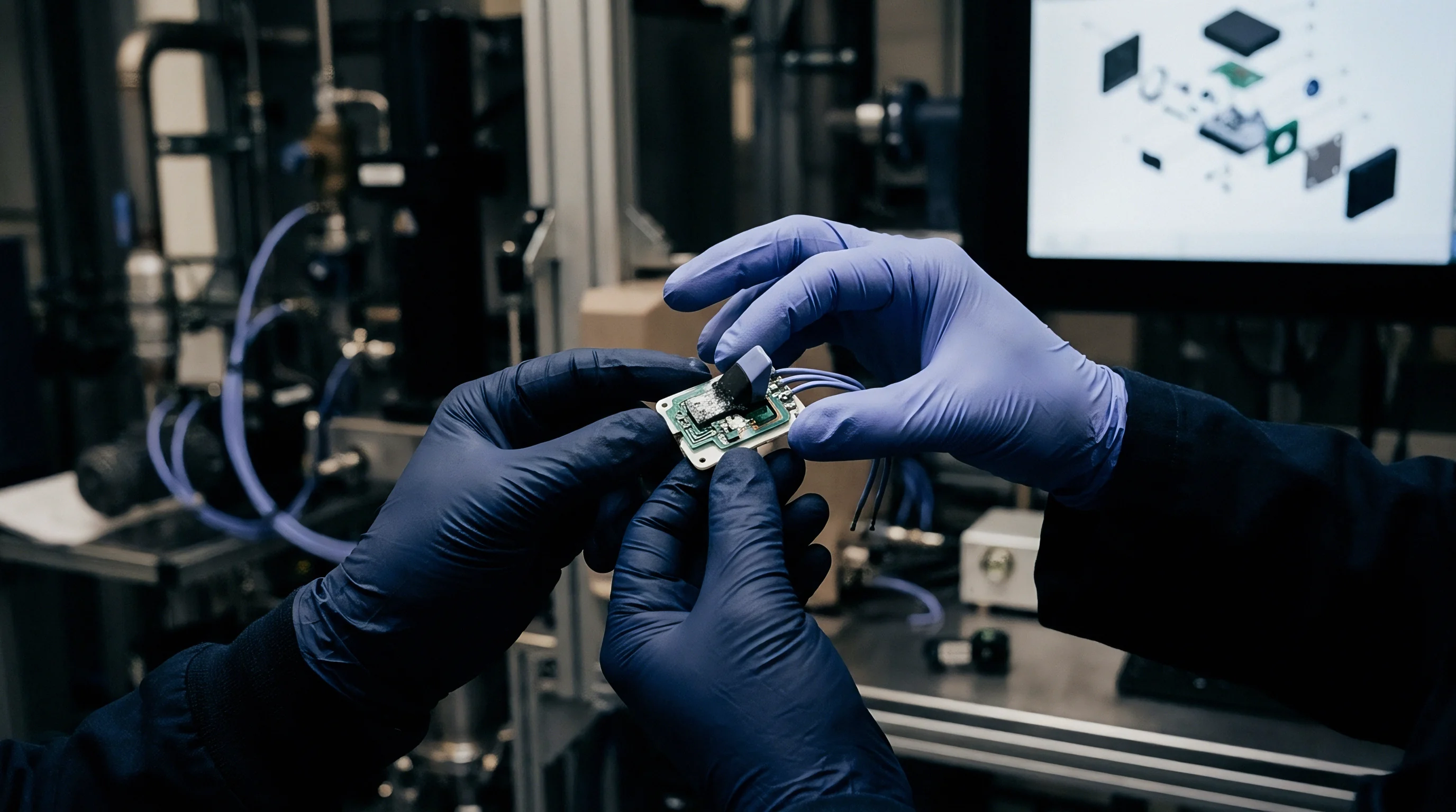
Quality control for complex stackups relies on destructive microsection coupons cut from panel margins. Fabrication drawings should explicitly require IPC-2221 test coupons designed to evaluate both rigid multi-layer plating and flex transition integrity. Microsection analysis verifies internal layer registration, drill accuracy, and resin containment.
Inspecting coupon microsections under optical and scanning electron microscopy uncovers structural defects invisible to automated optical inspection (AOI) or X-ray tools. Key evaluation points include plated-through hole wall thickness, inner-layer copper foil separation, resin recession behind plated barrels, and micro-voids in no-flow prepreg fill zones next to coverlay edges.
Quality Coupon Architecture for Flex-Rigid Boundaries
IPC coupons positioned in panel drop-outs record resin flow, drill registration, and plating quality across the transition zone. Coupon layouts for rigid-flex panels include blind and buried microvias alongside full-depth plated holes through both rigid FR-4 and flex polyimide cores. Testing thermal stress resistance involves floating coupons in solder at 288 degrees Celsius for 10 seconds before epoxy mounting and polishing.
IPC-6013 Class 3 standards set strict microsection acceptance limits. Plated-through hole copper must maintain a continuous average wall thickness of at least 25 microns (1.0 mil), with no individual spot below 20 microns. Internal annular rings in rigid sections require a minimum of 50 microns of solid copper around drilled holes after accounting for registration tolerances and drill wander.
- Cut microsection specimens from panel border coupons adjacent to the rigid-flex junction using a precision diamond saw.
- Mount specimens in thermosetting epoxy resin cured at room temperature to avoid thermal stress artifacts.
- Grind and polish mounted cross-sections through silicon carbide grit down to a 0.05 micron alumina slurry.
- Perform a chemical etch using ammonium hydroxide and hydrogen peroxide solution to reveal copper grain boundaries.
- Inspect sections under an optical microscope at 100x to 400x magnification against IPC-6013 Class 3 hole wall and etch criteria.
Fabrication Drawing Specification Notes
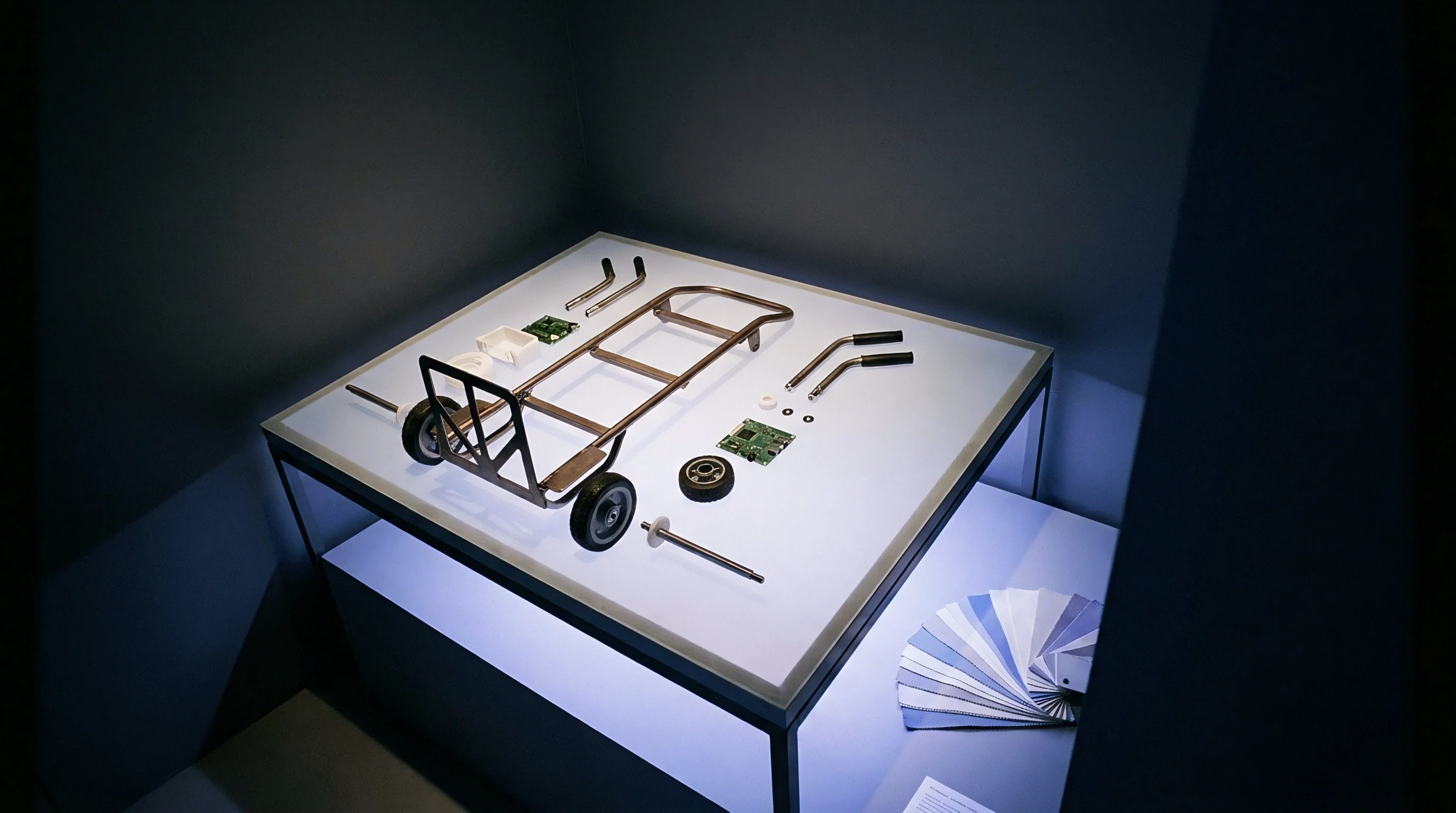
Fabrication drawings should include explicit notes governing material callouts, copper foil types, and repair criteria. Clear IPC callouts on artwork prevent fabricators from substituting lower-grade laminates or high-expansion adhesives in multi-layer rigid sections.
| Inspection Parameter | IPC-6013 Class 2 Requirement | IPC-6013 Class 3 Requirement | Defect Mechanism |
|---|---|---|---|
| PTH Copper Wall Thickness (Average) | Minimum 20 Microns | Minimum 25 Microns | Plating Void / Barrel Fracture |
| Polyimide-to-Prepreg Delamination | Max 1% of Interface Length | Zero Delamination Allowed | Thermal Expansion Shear Stress |
| Prepreg Resin Squeeze-Out | Maximum 2.5 mm Beyond Edge | Maximum 1.0 mm Beyond Edge | Excessive Lamination Flow |
| Internal Annular Ring Minimum | 90 Degree Breakout Permitted | Minimum 50 Microns Solid Copper | Drill Wander / Registration Shift |
Specifying IPC-6013 Class 3 compliance on fabrication drawings requires manufacturers to document thermal stress microsection data for every lamination lot, establishing traceability before bare boards hit the assembly line.