Dielectric Loss
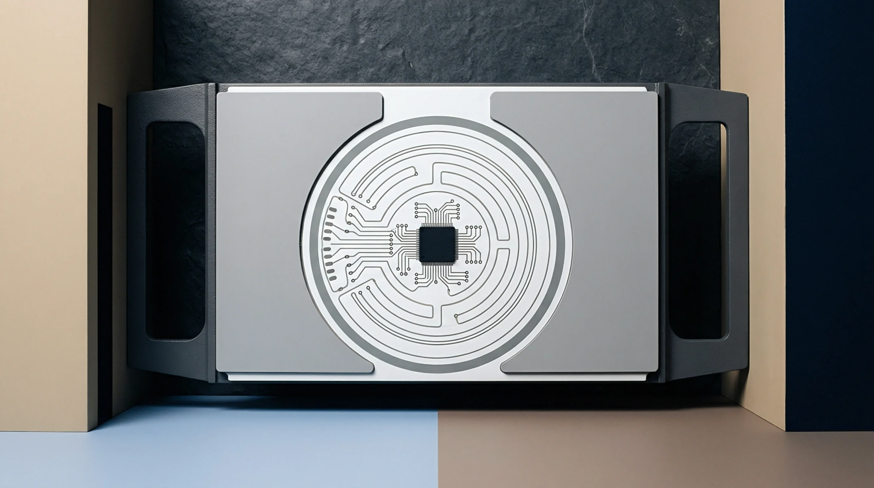
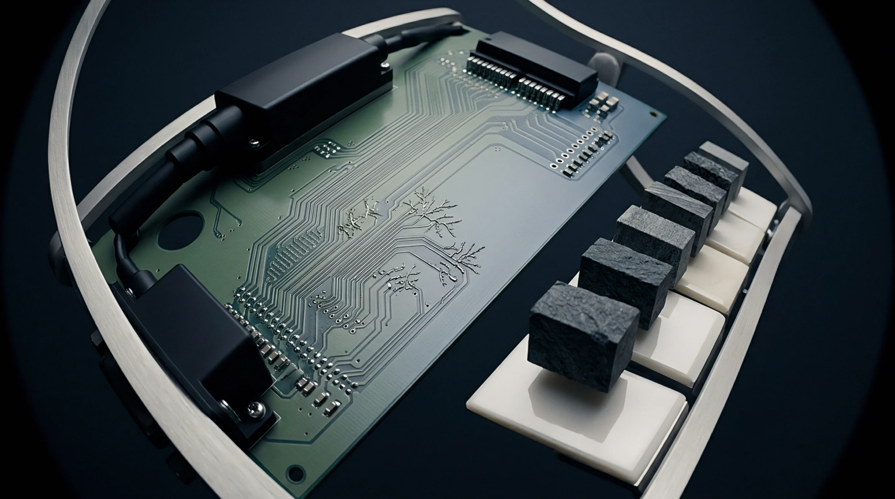
Dielectric energy conversion characterizes the internal behavior of insulating materials under oscillating electric fields. The dissipation factor quantifies the ratio of power lost as heat to the total power stored within the bulk dielectric of a printed circuit board. High values signal polar molecular structures or moisture absorption that convert alternating current into thermal energy rather than transmitting signals across the laminate substrate.
Industry standards define this metric as the tangent of the loss angle derived from the phase difference between applied voltage and resulting current. It governs signal integrity for high frequency digital and analog circuits where thermal buildup risks structural delamination or permanent shifts in impedance profiles across the frequency spectrum.
Material Performance
Signal attenuation across copper traces depends upon the base resin chemistry and fiberglass reinforcement within the laminate. A dissipation factor remains low for materials like polytetrafluoroethylene and polyimide compared to standard epoxy resins which exhibit higher losses due to chemical dipole rotation. Manufacturers select these substrates to minimize signal degradation during transmission through high density interconnects.
Variations in weave geometry or resin distribution introduce local fluctuations in the loss profile across a panel surface. Inspection involves swept frequency measurements using resonant cavity perturbations or split post dielectric resonators to verify that the manufactured board meets the electrical design specification. Each increase in the operating frequency forces tighter limits on this value because energy waste accumulates proportionally with the switching speed.
Control over this property preserves the amplitude of logic pulses traveling from drivers to receivers across long trace runs.
Measurement Protocol
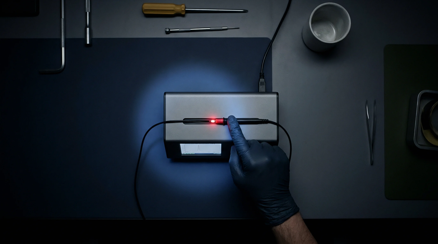
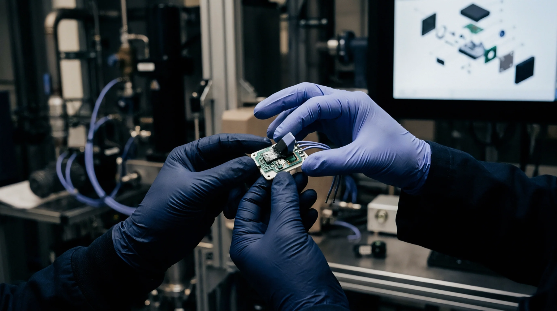
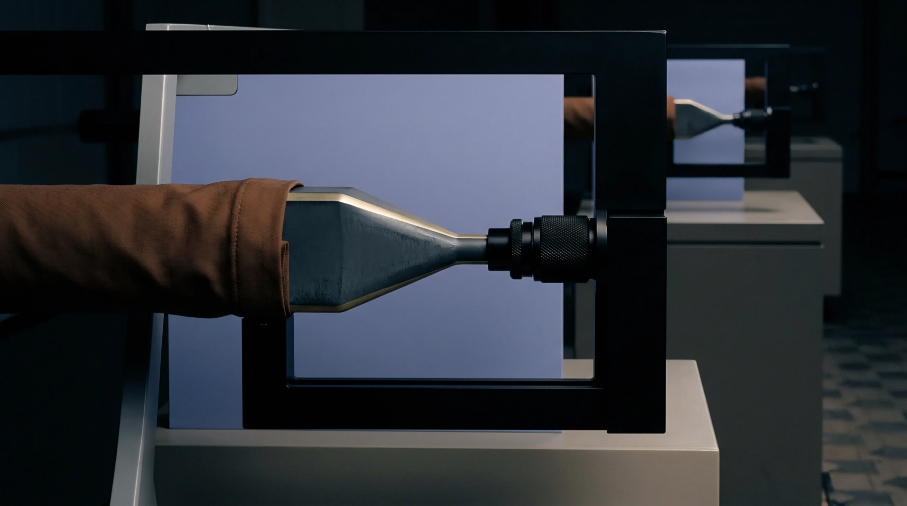
Vector network analyzers provide the necessary apparatus to determine the ratio of resistive loss to capacitive reactance. Engineers isolate the test coupon from the finished circuit board to eliminate parasitic inductance from components and solder joints. Accurate results require calibration against a reference material with known dielectric behavior under identical temperature and humidity conditions.
High resolution sensors detect minute deviations in the phase response that indicate contamination or improper polymerization during the lamination process. Any departure from the baseline value prevents the circuit from maintaining the target bandwidth. Dielectric energy dissipation predicts the operational limit of the final hardware.