Transmission Path
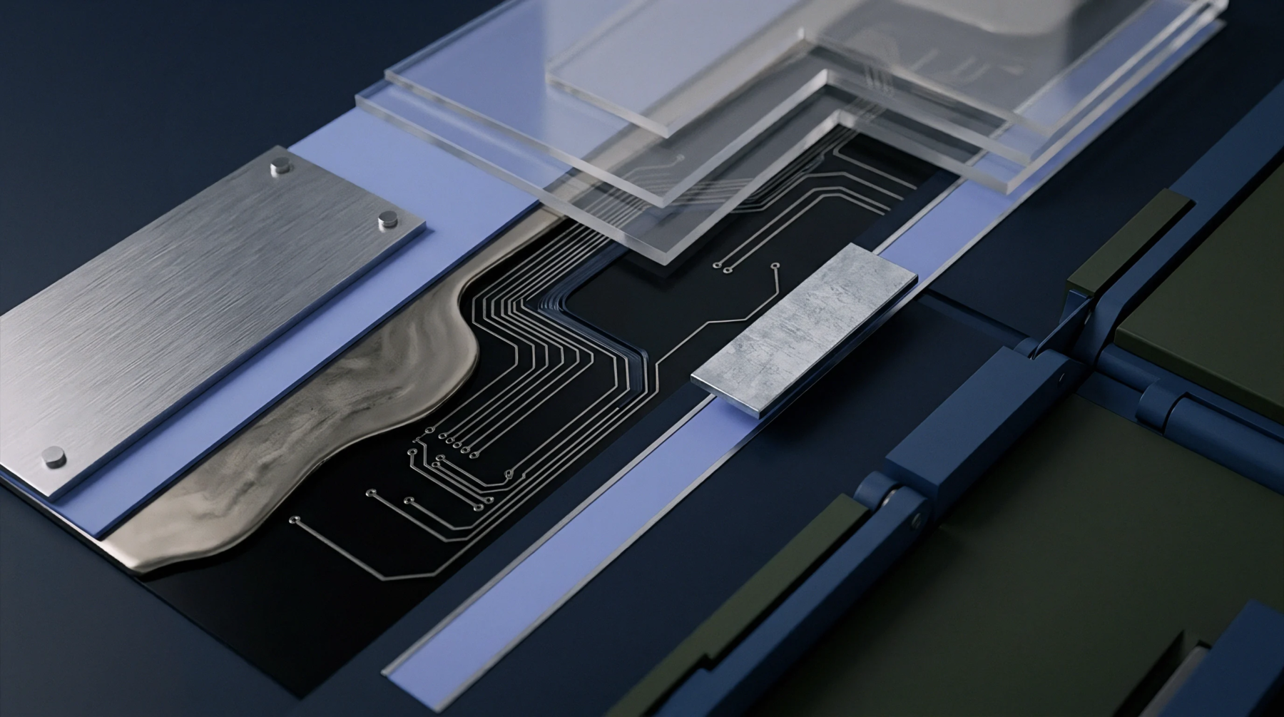
A stripline constitutes a planar transmission line configuration where a conductive ribbon remains sandwiched between two ground planes within a dielectric substrate. Electromagnetic energy travels through this central conductor, held in place by insulating material that separates the signal path from the outer shielding layers. Designers select this geometry to provide high isolation between adjacent circuits while managing electromagnetic interference in dense circuit board layouts.
The velocity of signal propagation depends upon the dielectric constant of the chosen material, which limits the bandwidth of the interconnect. Laminate manufacturers control the spacing between these layers to ensure a consistent impedance profile across the entire length of the conductive trace.
Fabrication Metric
Board shops calibrate etching processes to maintain the specific width of the stripline, as deviations alter the characteristic impedance of the finished assembly. Operators measure the copper thickness and dielectric height to verify that the trace performs according to the design specification. Impedance test equipment detects variations in the signal path by measuring reflections, which often arise from air gaps or resin voids in the material stack.
Failure to maintain symmetry between the top and bottom ground planes results in differential mode conversion that degrades signal integrity at high frequencies. Mechanical drilling of vias through these boards requires precise registration, otherwise the connection creates a parasitic capacitance that disrupts the intended electrical environment. Engineers define the allowable tolerance for these geometric parameters to prevent data errors in high speed digital modules.
Performance Constraint
Precise control of the termination environment dictates the effectiveness of the stripline, because any discontinuity produces signal degradation. Surface mount components attached to the board surface must transition through vias to reach the internal layer, introducing potential inductive load variations. Proper grounding strategies along these vertical transitions suppress common mode noise that would otherwise radiate from the board edges.
When designers account for skin effect losses, they accurately predict the attenuation that occurs over the full trace length. This layout strategy remains the primary method for containing electromagnetic fields within the physical footprint of the printed circuit board.