SMT Reflow Temperature Profiling and Defect Analysis for Lead Free Assemblies
Optimized lead-free reflow profiling requires thermal deltas under eight degrees, controlled time above liquidus, and precise paste transfer efficiency.
Dynamics
Thermal Phase Boundaries in Lead Free Soldering
Lead-free assembly requires strict thermal control to convert solder paste into solid metallurgical joints. Moving from eutectic tin-lead to near-eutectic tin-silver-copper alloys raised melting thresholds by thirty to forty degrees Celsius. SAC305, composed of ninety-six point five percent tin, three percent silver, and zero point five percent copper, has a liquidus temperature of two hundred seventeen degrees Celsius.
Achieving reliable wetting calls for peak reflow temperatures between two hundred thirty-five and two hundred forty-five degrees Celsius across every joint on a board. That usable process window shrinks quickly when high-density components sit next to large copper planes or heat sinks.
Thermal profiling traces the temperature curve of the assembly as it passes through the reflow oven zones. The profile breaks into four distinct phases: preheat, soak, reflow above liquidus, and cooling. Each zone drives specific chemical and physical reactions between the solder paste deposit and component terminations.
Heating too rapidly causes thermal shock, component cracking, and solvent spatter. Insufficient heat fails to activate the flux, leaving surface oxides intact and preventing full metal coalescence.
The preheat phase raises the assembly from ambient temperature to roughly one hundred fifty degrees Celsius, using heating rates between one point zero and two point zero degrees Celsius per second. Linear ramp profiles maintain a steady rise directly toward liquidus to minimize thermal exposure. Target ramp profiles instead insert an isothermal soak between one hundred fifty and one hundred eighty degrees Celsius for sixty to one hundred twenty seconds.
This soak levels out temperature differences across panels carrying mixed-technology components before they enter the reflow zone.
| Alloy Formulation | Liquidus Temp (°C) | Max Preheat Ramp (°C/s) | Soak Window (°C / s) | Time Above Liquidus (s) | Peak Temperature Range (°C) | Cooling Ramp Limit (°C/s) |
|---|---|---|---|---|---|---|
| SAC305 (Sn96.5Ag3.0Cu0.5) | 217 | 2.0 | 150 – 180 / 60 – 100 | 45 – 75 | 235 – 245 | -4.0 |
| SAC105 (Sn98.5Ag1.0Cu0.5) | 217 – 227 | 1.5 | 160 – 190 / 60 – 120 | 50 – 80 | 240 – 250 | -3.0 |
| SN100C (Sn99.3Cu0.7+Ni+Ge) | 227 | 1.5 | 150 – 180 / 60 – 90 | 45 – 70 | 245 – 255 | -4.0 |
| Bi58Sn42 (Low Temp) | 138 | 1.5 | 90 – 110 / 30 – 60 | 40 – 60 | 165 – 180 | -3.0 |
Liquidus Kinetics and Peak Heat Exposure
Time above liquidus is how long the solder stays completely molten. For SAC305, this window runs between forty-five and seventy-five seconds. Sufficient time above liquidus lets the flux clear remaining oxides, aids liquid metal wetting, and gives volatile reaction products time to outgas from the joint.
Pushing time above liquidus beyond ninety seconds thickens the intermetallic compound layer at the copper-solder interface. When that intermetallic layer exceeds four micrometers, it creates a brittle plane vulnerable to mechanical shock.
A soak duration under sixty seconds leaves large thermal deltas uncorrected across thick multilayer boards.
Peak reflow temperature balances void evacuation against thermal damage to substrates or sensitive active devices. Under J-STD-020 requirements, maximum component body temperatures cannot exceed two hundred sixty degrees Celsius. Low-mass components like 0201 passives heat up rapidly, while ball grid arrays sitting over heavy copper ground planes lag behind.
Profilers place calibrated thermocouples directly on the highest and lowest mass joints to track this gap. The maximum allowable temperature differential across the assembly at peak reflow is eight degrees Celsius.
Controlled cooling sets the final grain size of the solder joint. Standard cooling ramps run between two and four degrees Celsius per second. Rapid cooling forms a fine-grained microstructure with strong fatigue resistance and smaller silver-tin intermetallic precipitates.
Cooling slower than one point five degrees Celsius per second yields coarse grain structures, larger voids, and poor creep resistance. Conversely, cooling faster than six degrees Celsius per second risks cracking ceramic chip capacitors from thermal strain and delaminating the substrate. Drifting outside these thermal boundaries leads to line stops, scrap, and ruined circuit boards.
Deposit

Stencil Aperture Mechanics and Transfer Efficiency
Paste printing sets the initial volume of metal available for every solder joint. Transfer efficiency is the ratio of actual deposited solder paste volume to the theoretical volume of the stencil aperture. In fine-pitch applications, that efficiency depends on the area ratio ~ calculated by dividing the aperture floor area by the aperture wall area.
For reliable paste release with electro-polished laser-cut stainless steel stencils, the area ratio must exceed zero point six six. Nano-coated stencils can maintain consistent release down to zero point five five.
Type 4 solder paste, with sphere diameters from twenty to thirty-eight micrometers, works for aperture sizes down to two hundred micrometers. Printing onto zero point four millimeter pitch micro-BGA pads requires Type 5 paste, which uses particle distributions between fifteen and twenty-five micrometers. Poor paste release leaves thin joints, open circuits, and weak fillets.
Too much paste leads to bridging, solder beads, and mid-chip balling during reflow.
- Aperture area ratio sets the physical limit for paste release through thin laser-cut stencil walls as the board separates.
- Solder paste rheology determines how quickly viscosity recovers once squeegee shear stress stops across the stencil.
- Squeegee blade pressure ensures clean stencil wiping without scooping paste out of wide apertures.
- Separation speed profile prevents deposit tailing and edge slump before component placement.

Paste Volatility and Thermal Coalescence
Solder paste is metal powder suspended in a liquid vehicle of solvents, resins, activators, and thixotropic agents. This organic vehicle makes up roughly fifty percent of the deposited paste volume, though only ten percent of its mass. Volatile solvents evaporate during preheat; if heating happens too fast, boiling solvent can violently blow solder particles onto the surrounding mask, leaving permanent solder balls after reflow.
Type 4 powder requires an area ratio above zero point six six to achieve eighty percent transfer efficiency.
Flux activation starts as temperatures cross one hundred thirty degrees Celsius, where organic acids reduce surface oxides on component leads, board pads, and the solder powder itself. Cleaned metal surfaces lower interfacial tension, letting molten solder flow and wet evenly. If flux activity is insufficient, solder powder spheres fail to melt into a single continuous volume ~ a condition called incomplete coalescence.
The result is a grainy, unbonded deposit that breaks under slight mechanical stress. Maintaining stable paste volume remains critical to high-yield surface mount assembly.
Failure
Kinetic and Surface Tension Defect Mechanisms
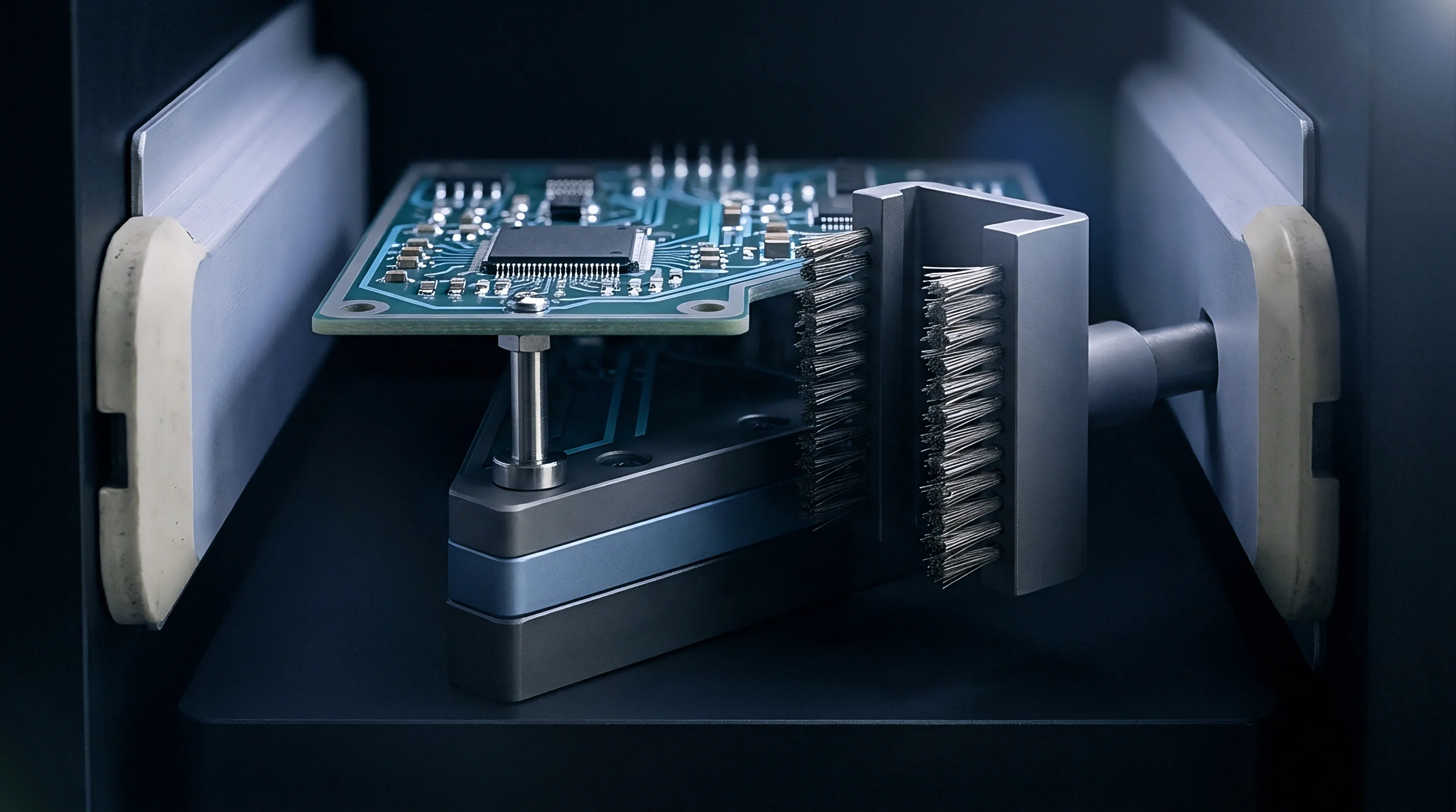
Thermal gradients and unbalanced surface tension drive distinct physical defect modes in lead-free reflow. Tombstoning happens mainly on two-terminal passives when one pad reaches liquidus before the other. Solder paste on the hotter pad melts first, pulling the un-melted end of the component vertical.
Mismatched paste volumes, asymmetric trace widths, and temperature imbalances across the oven tunnel aggravate the problem. Matching trace geometries to balance heat flow into nearby ground planes reduces these melting delays.
Head-in-pillow defects occur on area array packages, especially large fine-pitch BGAs, due to thermal warping of the package substrate or circuit board during preheat. As the package bows upward, its solder spheres lift away from the paste deposit on the board. Oxides then form a thin skin over both molten surfaces.
When the board cools and flattens again, the sphere presses back against the paste deposit but cannot coalesce, leaving two separate, unbonded surfaces touching.
| Defect Classification | Primary Physical Root Cause | Thermal Profile Factor | Stencil / Print Factor | Corrective Action Focus |
|---|---|---|---|---|
| Tombstoning | Asymmetrical surface tension torque | Excessive preheat ramp rate | Unequal deposit volumes | Equalize pad thermal mass, soak extended |
| Head-in-Pillow (HiP) | Package dynamic warpage during reflow | High thermal delta across package | Insufficient paste height | Lower peak temp, adjust soak zone |
| BTC Voiding (>25%) | Outgassing of flux volatiles trapped under die | Short time above liquidus | Solid coverage stencil design | Implement windowpane stencil pattern |
| Solder Bridging | Molten solder bridging adjacent conductors | Excessive peak heat soak | Over-printing, aperture misalign | Reduce aperture area, check alignment |
| Mid-Chip Balling | Paste squeeze-out under component body | Fast preheat solvent boiling | Excessive deposit thickness | Reduce aperture width, add side-notches |
Outgassing and Interfacial Void Formation
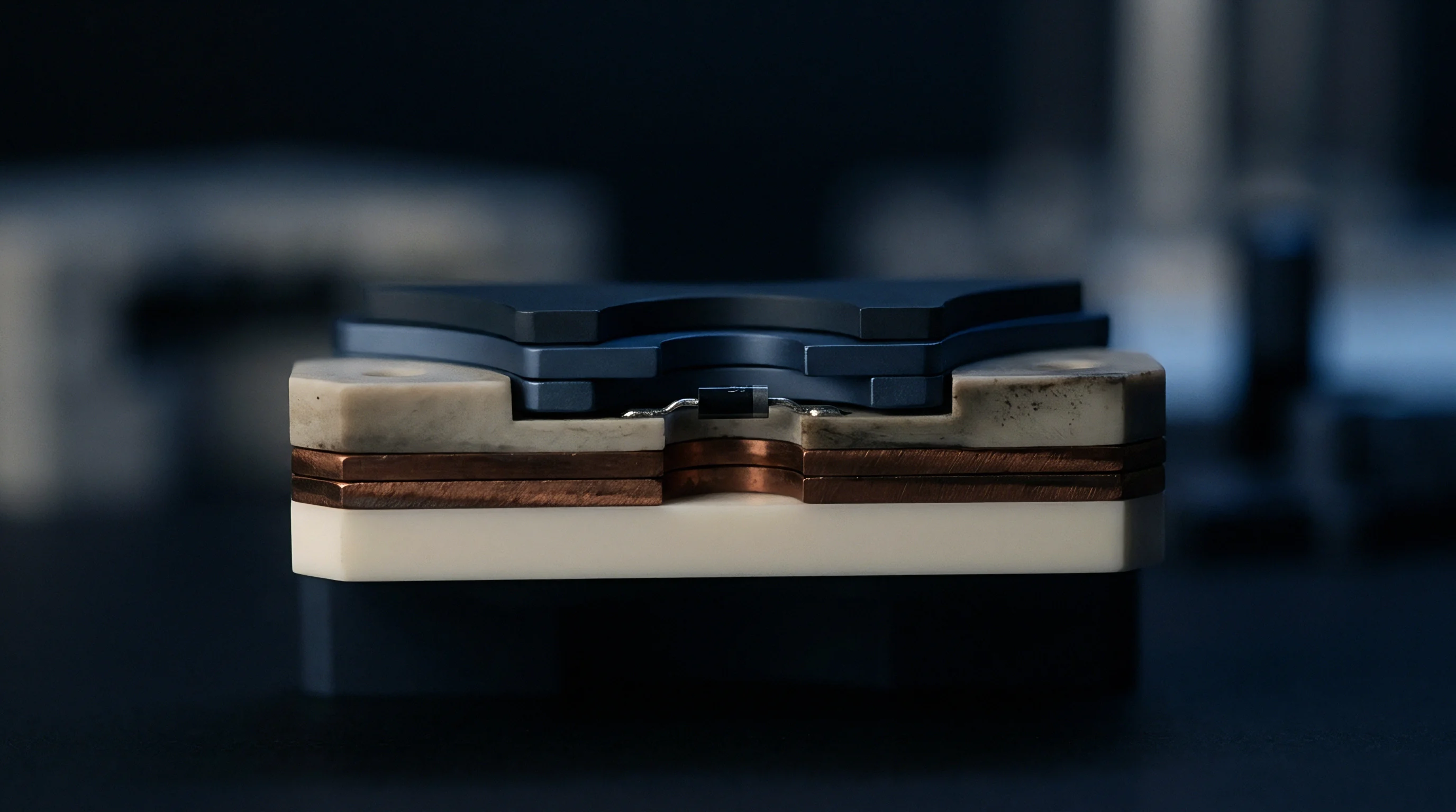
Voids inside solder joints degrade electrical conductivity, thermal pathing, and mechanical strength. Bottom-terminated components like quad-flat no-leads packages and power MOSFETs are especially prone to voiding under their central thermal pads. Volatiles from the flux get trapped beneath the broad package during fast reflow, frozen in place before they can escape.
Under IPC-A-610 Class 3 standards, thermal pad voiding must stay below twenty-five percent of the joint area.
Executing systematic root-cause diagnosis requires an ordered, evidence-based sequence on the shop floor.
- Inspect board layout files to verify thermal pad land geometries and copper balance across adjacent layers.
- Review solder paste inspection volumetric data to confirm deposit height uniformity across suspect component locations.
- Record real-time reflow profiles with a calibrated, board-mounted thermocouple logger placed at the defect site.
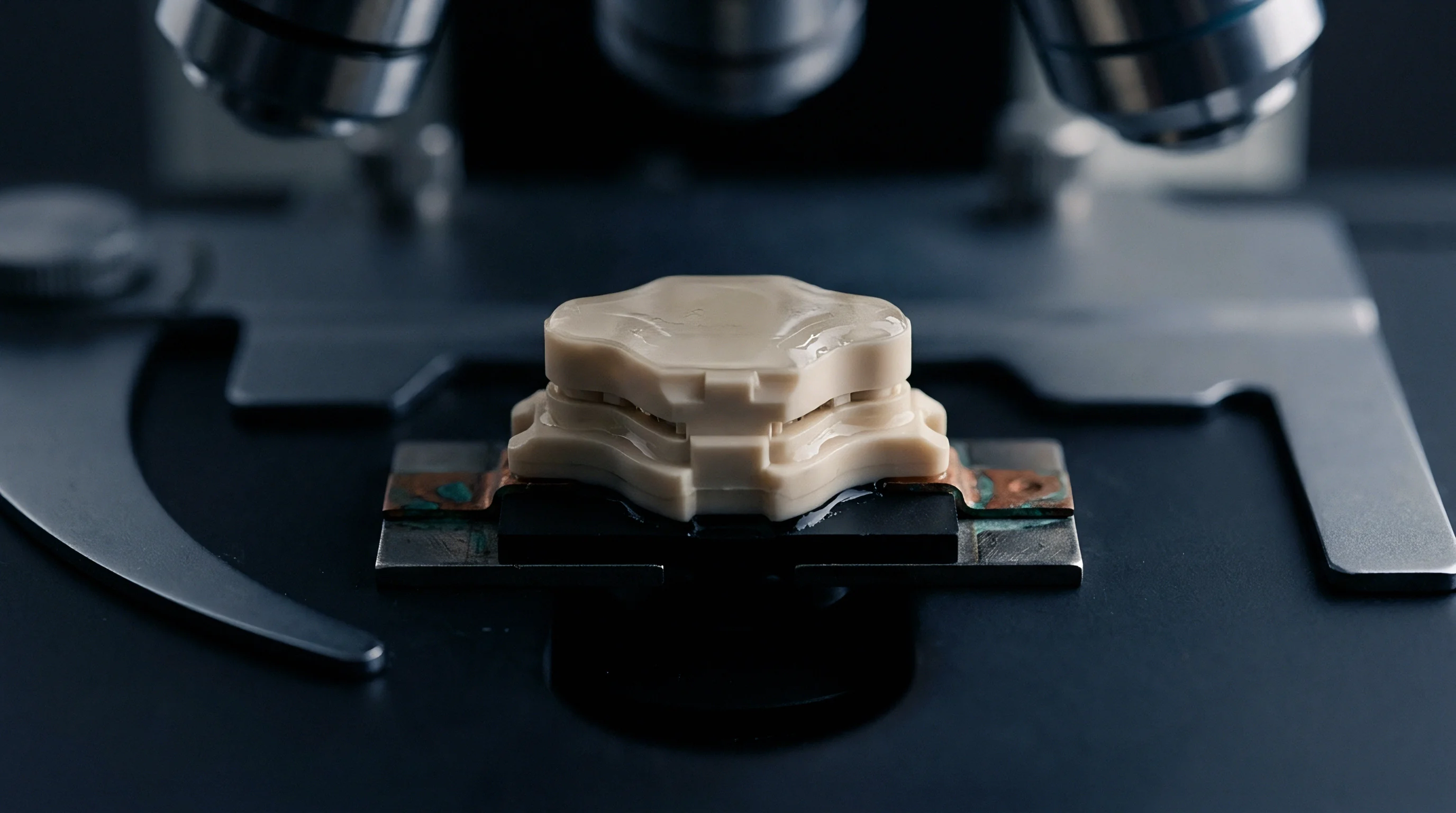
- Cross-section selected failed joints to examine intermetallic layer thickness and crystal structure under microscopic imaging.
- Adjust stencil aperture patterns or oven zone setpoints using the physical evidence gathered from microsection analysis.
Pad cratering creates micro-fractures in the resin-glass matrix directly below copper bond pads. Higher lead-free reflow temperatures increase thermal expansion stress on the substrate. As the board cools, the stiffness of SAC305 channels mechanical strain straight into the rigid epoxy laminate.
Because these micro-fractures stay hidden from visual checks, detecting them requires acoustic microscopy or dye-and-pry testing. Whether alternative low-silver alloys can reduce board strain without sacrificing thermal fatigue resistance remains a key question.
Inspection
Optical and Radiographic Verification Boundaries
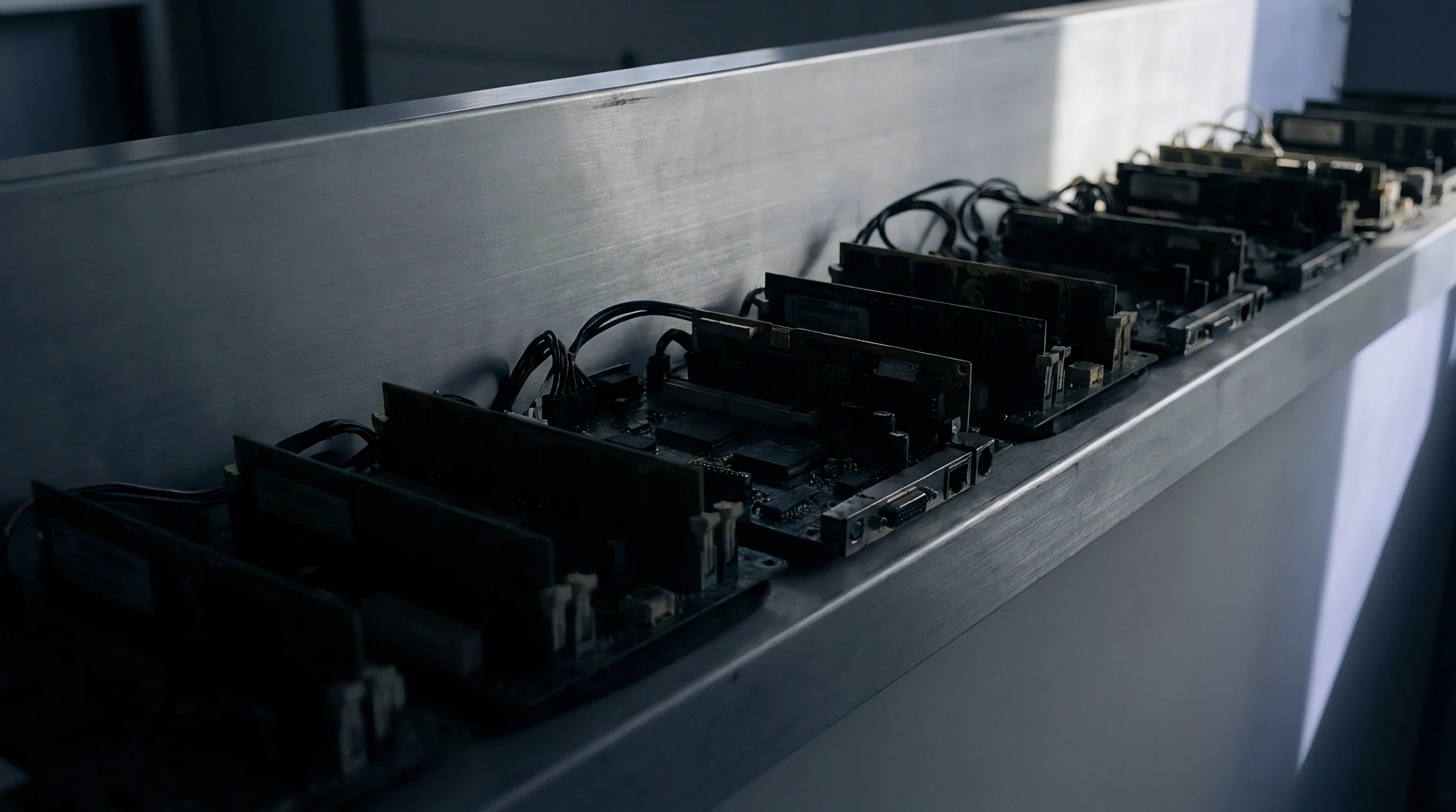
Automated optical inspection systems evaluate surface geometries, fillet contours, and component alignment using multi-angle light arrays. They reliably catch bridging, missing parts, tombstoning, and insufficient surface solder. However, optical inspection cannot see hidden joint structures under area array packages, bottom-terminated devices, or shield cans.
Relying on optical checks alone leaves internal structural defects undetected on high-density boards.
Transmission X-ray inspection checks hidden joints by measuring radiation absorption through materials of differing density. High-tin lead-free alloys absorb X-rays less readily than traditional tin-lead solders, requiring adjustments to tube voltage and exposure settings. Three-dimensional computed laminography reconstructs cross-sectional slices through BGA spheres, isolating top-side joint structures from bottom-side components on double-sided assemblies.
These algorithms calculate void percentages, pinpoint head-in-pillow faults, and detect internal micro-voids in hidden solder joints.
What Escapes Automated Optical Check under Bottom Terminated Devices?
Quad-flat no-lead side termination fillets often show inconsistent wetting even when the electrical connection underneath is sound. Automated optical systems flag these incomplete toe fillets on QFN edge pads, causing false-call rates above fifteen percent on high-volume lines. Operators routinely override those flags, which increases the risk of overlooking genuine non-wetting beneath the hidden thermal pad.
X-ray inspection picks up voids under QFN centers, but cannot verify whether peripheral signal pins have achieved proper wetting without micro-sectioning.
IPC-A-610 Class 3 mandates that voiding within thermal pad solder joints must not exceed twenty-five percent of the total area.
Operators often blame unverified joint defects on lead oxidation or degraded board finishes. False-call handling rules require physical secondary verification before any override is allowed. Setting optical inspection sensitivity too high leads to operator fatigue and missed defects.
To keep defect detection reliable on production runs, false calls must stay below zero point five percent.
Protocol

Thermocouple Instrumentation and Profile Validation
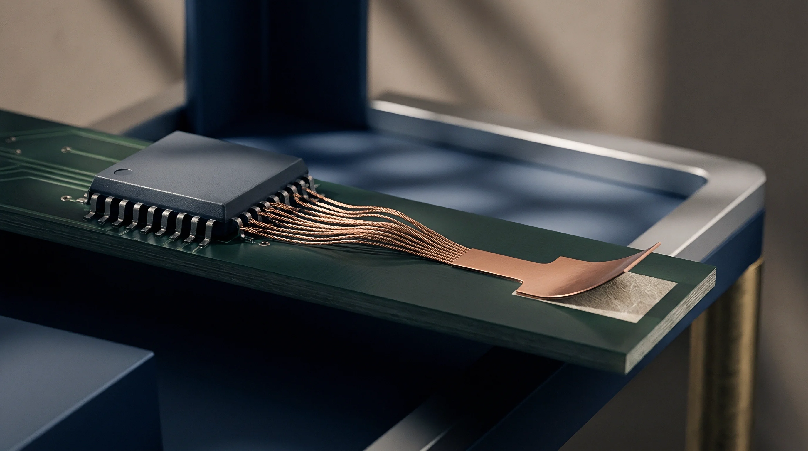
Line qualification requires thorough thermal profiling before running production panels. Profiling runs must use an actual production board wired with high-temperature K-type thermocouples. Junctions are attached with high-temperature silver epoxy or micro-soldering to ensure direct contact with critical component terminals.
Sensors left hanging in open air or held with Kapton tape produce inaccurate readings, invalidating the run.
Sensors are placed on the heaviest components, the smallest passives, and central array joints, while trailing thermocouples track ambient tunnel temperatures to verify heating zone stability. The recorded thermal trace must demonstrate that all sensors stay within the process window parameters set by component and paste manufacturers. Operators log these profile files directly against specific board assemblies in the factory management system.
Line release proceeds only after completing a structured qualification checklist for the specific assembly run.
- Thermocouple calibration check confirms sensor readings match within zero point five degrees Celsius in a reference bath.
- Profiling board validation ensures attachment points capture the true thermal spread between high-mass and low-mass components.
- Paste deposit logging records paste lot numbers, ambient room temperature, and relative humidity before printing.
- First-article x-ray check measures voiding on all bottom-terminated devices against Class 3 limits.
- Oven thermal stability audit verifies heating zone temperatures stay within one degree Celsius of setpoints under load.
IPC-J-STD-001 Section 4.5 mandates written process control records for all automated soldering equipment used in Class 3 builds. Compliance depends on real-time data logs recorded during setup. Missing or incomplete profiling logs void assembly qualification and invalidate lot acceptance under military or medical contracts.


Outturn
Commercial Impact of Process Window Deviations
Profiling errors directly hit manufacturing costs, line throughput, and unit profitability. Operating outside the paste window inflates defect rates and forces manual rework. Touch-ups on fine-pitch parts introduce localized thermal stress, degrade surrounding laminate resin, and double labor costs on those units.
When first-pass yield falls below ninety-two percent, mandatory line holds kick in, consuming margin through scrap and troubleshooting.
Setup time is a significant fixed cost in surface mount assembly. Profiling a complex double-sided lead-free board takes two to four hours of dedicated line capacity. Rushing setup to save money risks hidden defects, customer returns, and costly field failures.
Sourcing contracts should clearly define who pays for profile optimization setup versus scrap generated during line setup.
| Profile Quality Level | First Pass Yield (%) | Rework Hours per 1k Units | Scrap Rate (%) | Cost Impact per Unit ($) |
|---|---|---|---|---|
| Optimized Process Window | 98.5 | 4.0 | 0.2 | Base Quoted Price |
| Unbalanced Delta (8-12°C) | 92.0 | 22.0 | 1.5 | + 8.50 |
| Inadequate TAL (<40s) | 84.0 | 48.0 | 3.8 | + 19.20 |
| Excessive Peak (>255°C) | 76.0 | 12.0 (High Scrap) | 8.5 | + 34.00 |
Contract manufacturing agreements typically limit liability for component damage during assembly. Assemblers absorb internal scrap up to an agreed threshold, usually zero point five percent of total placement counts. However, defects traced to unvalidated reflow profile changes shift full financial liability back to the contract manufacturer.
Detailed defect analysis records provide the evidence needed during yield disputes.
Process profile deviations directly increase labor cost per assembly through secondary manual rework passes.
Repeat reflow cycles and localized rework heat drive continued intermetallic layer growth in existing joints. Re-exposing SAC305 joints to peak temperatures above two hundred thirty degrees Celsius thickens the copper-tin intermetallic layer by zero point five to one point two micrometers per pass. Excessive growth makes the joint brittle, compromising vibration resistance and thermal fatigue life in military and automotive hardware.
In the end, profile validation is what stands between quoted board margins and field reliability.